
Datasheet


10
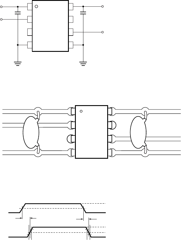
Application Information
Bypassing and PC Board Layout
The HCPL-7723/0723 optocouplers are extremely easy to
use. No external interface circuitry is required because
the HCPL-7723/0723 use high-speed CMOS IC technol-
ogy allowing CMOS logic to be connected directly to the
inputs and outputs.
As shown in Figure 1, the only external components
required for proper operation are two bypass capacitors.
Capacitor values should be between 0.01 µF and 0.1 µF.
For each capacitor, the total lead length between both
ends of the capacitor and the power-supply pins should
not exceed 20 mm. Figure 2 illustrates the recommended
printed circuit board layout for the HCPL-7723/0723.
Figure 3. Timing diagram to illustrate propagation delay, tplh and tphl.
INPUT
t
PLH
t
PHL
OUTPUT
V
I
V
O
10%
90%90%
10%
V
OH
V
OL
0 V
50%
5 V CMOS
2.5 V CMOS
Figure 1. Functional diagram.
Figure 2. Recommended printed circuit board layout.
Propagation Delay, Pulse-Width Distortion and Propa-
gation Delay Skew
Propagation Delay is a gure of merit which describes
how quickly a logic signal propagates through a system
as illustrated in Figure 3. The propagation delay from low
to high (t
PLH
) is the amount of time required for an input
signal to propagate to the output, causing the output to
change from low to high. Similarly, the propagation delay
from high to low (t
PHL
) is the amount of time required for
the input signal to propagate to the output, causing the
output to change from high to low.
7
5
6
8
2
3
4
1
GND
2
C1 C2
NC
V
DD2
NC
V
O
V
DD1
V
I
720
YWW
C1, C2 = 0.01 µF TO 0.1 µF
GND
1
V
DD2
C1 C2
720
YWW
V
O
GND
2
V
DD1
V
I
GND
1
C1, C2 = 0.01 µF TO 0.1 µF