
Datasheet


For product information and a complete list of distributors, please go to our website: www.avagotech.com
Avago, Avago Technologies, and the A logo are trademarks of Avago Technologies Limited in the United States and other countries.
Data subject to change. Copyright © 2005-2008 Avago Technologies Limited. All rights reserved. Obsoletes AV01-0551EN
AV02-1360EN - June 20, 2008
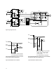
IPM Dead Time and Propagation Delay Specications
The HCPL-4506 series include a Propagation Delay Dier-
ence specication intended to help designers minimize
“dead time” in their power inverter designs. Dead time is
the time period during which both the high and low side
power transistors (Q1 and Q2 in Figure 24) are o. Any
overlap in Q1 and Q2 conduction will result in large cur-
rents owing through the power devices between the
high and low voltage motor rails.
To minimize dead time the designer must consider the
propagation delay characteristics of the optocoupler
as well as the characteristics of the IPM IGBT gate drive
circuit. Considering only the delay characteristics of the
optocoupler (the characteristics of the IPM IGBT gate
drive circuit can be analyzed in the same way) it is impor-
tant to know the minimum and maximum turn-on (t
PHL
)
and turn-o (t
PLH
) propagation delay specications, pref-
erably over the desired operating temperature range.
The limiting case of zero dead time occurs when the in-
put to Q1 turns o at the same time that the input to
Q2 turns on. This case determines the minimum de-
lay between LED1 turn-o and LED2 turn-on, which
is related to the worst case optocoupler propagation
delay waveforms, as shown in Figure 25. A minimum
dead time of zero is achieved in Figure 25 when the
signal to turn on LED2 is delayed by (t
PLH max
- t
PHL
min
) from the LED1 turn o. Note that the propagation
delays used to calculate PDD are taken at equal tem-
peratures since the optocouplers under consideration
are typically mounted in close proximity to each other.
(Specically, t
PLH max
and t
PHL min
in the previous equa-
tion are not the same as the t
PLH max
and t
PHL min
, over the
full operating temperature range, specied in the data
sheet.) This delay is the maximum value for the propaga-
tion delay dierence specication which is specied at
450 ns for the HCPL-4506 series over an operating tem-
perature range of
-40°C to 100°C.
Delaying the LED signal by the maximum propagation
delay dierence ensures that the minimum dead time
is zero, but it does not tell a designer what the maxi-
mum dead time will be. The maximum dead time oc-
curs in the highly unlikely case where one optocoupler
with the fastest t
PLH
and another with the slowest t
PHL
are in the same inverter leg. The maximum dead
time in this case becomes the sum of the spread
in the t
PLH
and t
PHL
propagation delays as shown in Figure 26.
The maximum dead time is also equivalent to the dier-
ence between the maximum and minimum propagation
delay dierence specications. The maximum dead time
(due to the optocouplers) for the HCPL-4506 series is
600 ns (= 450
ns - (-150 ns) ) over an operating tempera-
ture range of -40°C to 100°C.