
Datasheet

11
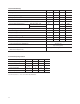
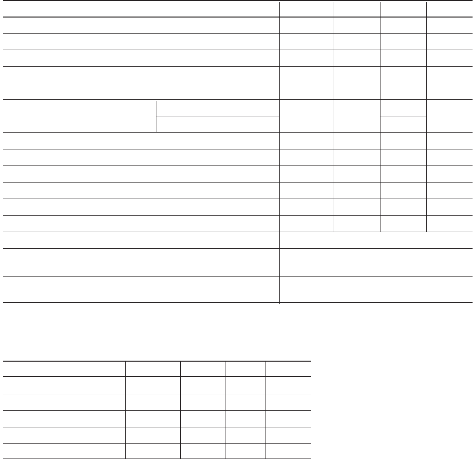
Absolute Maximum Ratings
Parameter Symbol Min. Max. Units
Storage Temperature T
S
-55 125 °C
Operating Temperature T
A
-40 100 °C
Average Input Current
[1]
I
F(avg)
25 mA
Peak Input Current
[2]
(50% duty cycle, ≤1 ms pulse width) I
F(peak)
50 mA
Peak Transient Input Current (<1 µs pulse width, 300 pps) I
F(tran)
1.0 A
Reverse Input Voltage (Pin 3-2) HCPL-4506, HCPL-0466 V
R
5 Volts
HCPL-J456, HCNW4506 3
Average Output Current (Pin 6) I
O(avg)
15 mA
Resistor Voltage (Pin 7) V
7
-0.5 V
CC
Volts
Output Voltage (Pin 6-5) V
O
-0.5 30 Volts
Supply Voltage (Pin 8-5) V
CC
-0.5 30 Volts
Output Power Dissipation
[3]
P
O
100 mW
Total Power Dissipation
[4]
P
T
145 mW
Lead Solder Temperature (HCPL-4506, HCPL-J456) 260°C for 10 s, 1.6 mm below seating plane
Lead Solder Temperature (HCNW4506) 260°C for 10 s
(up to seating plane)
Infrared and Vapor Phase Reow Temperature See Package Outline Drawings Section
(HCPL-0466 and Option 300)
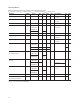
Recommended Operating Conditions
Parameter Symbol Min. Max. Units
Power Supply Voltage V
CC
4.5 30 Volts
Output Voltage V
O
0 30 Volts
Input Current (ON) I
F(on)
10 20 mA
Input Voltage (OFF) V
F(o)
* -5 0.8 V
Operating Temperature T
A
-40 100 °C
*Recommended V
F(OFF)
= -3 V to 0.8 V for HCPL-J456, HCNW4506.