
Datasheet


5
AbsoluteMaximumRatings
Parameter Symbol Min. Max. Units Note
Storage Temperature T
S
-55 125 °C
Junction Temperature T
J
-40 125 °C
Average Input Current I
F(AVG)
25 mA 1
Peak Transient Input Current I
F(TRAN)
1.0 A
(<1 µs pulse width, 300 pps)
Reverse Input Voltage V
R
5 V
“High” Peak Output Current I
OH(PEAK)
2.5 A 2
“Low” Peak Output Current I
OL(PEAK)
2.5 A 2
Supply Voltage V
CC
-V
EE
-0.5 25 V
Output Voltage V
O(PEAK)
0 V
CC
V
Output Power Dissipation P
O
250 mW 3
Total Power Dissipation P
T
295 mW 4
Lead Solder Temperature 260°C for 10 sec., 1.6 mm below seating plane
Solder Reflow Temperature Profile See Package Outline Drawings section
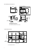
OUTPUT POWER – P
S
, INPUT CURRENT – I
S
0
0
T
S
– CASE TEMPERATURE – °C
200
600
400
25
800
50 75 100
200
150 175
P
S
(mW)
125
100
300
500
700
I
S
(mA)
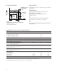
InsulationandSafetyRelatedSpecications
Parameter Symbol HCPL-3180 Units Conditions
Minimum External Air Gap L(101) 7.1 mm Measured from input terminals to output
(Clearance) terminals, shortest distance through air.
Minimum External Tracking L(102) 7.4 mm Measured from input terminals to output
(Creepage) terminals, shortest distance path along body.
Minimum Internal Plastic Gap 0.08 mm Through insulation distance conductor to
(Internal Clearance) conductor, usually the straight line distance
thickness between the emitter and detector.
Tracking Resistance CTI >175 V DIN IEC 112/VDE 0303 Part 1
(Comparative Tracking Index)
Isolation Group IIIa Material Group (DIN VDE 0110, 1/89, Table 1)
Note: Option 300 – surface mount classification is Class A in accordance with CECC 00802.