
Datasheet


15
Selecting the Gate Resistor (Rg) to Minimize IGBT Switching Losses.
Step 1: Calculate Rg Minimum From the I
OL
Peak Specication. The
IGBT and Rg in Figure 26 can be analyzed as a simple RC
circuit with a voltage supplied by the HCPL-3150/315J.
(V
CC
– V
EE
- V
OL
)
Rg ≥
I
OLPEAK
(V
CC
– V
EE
- 1.7 V)
=
I
OLPEAK
(15 V + 5 V - 1.7 V)
=
0.6 A
= 30.5 Ω
The V
OL
value of 2 V in the previous equation is a con-
servative value of V
OL
at the peak current of 0.6 A (see
Figure 6). At lower Rg values the voltage supplied by the
HCPL-3150/315J is not an ideal voltage step. This results
in lower peak currents (more margin) than predicted by
this analysis. When negative gate drive is not used V
EE
in
the previous equation is equal to zero volts.
Step 2: Check the HCPL-3150/315J Power Dissipation and Increase Rg
if Necessary. The HCPL-3150/315J total power dissipation
(P
T
) is equal to the sum of the emitter power (P
E
) and the
output power (P
O
):
P
T
= P
E
+ P
O
P
E
= I
F
•
V
F
•
Duty Cycle
P
O
= P
O(BIAS)
+ P
O (SWITCHING)
= I
CC
•
(V
CC
- V
EE
) + E
SW
(R
G
, Q
G
)
•
f
For the circuit in Figure 26 with I
F
(worst case) = 16 mA,
Rg = 30.5 Ω, Max Duty Cycle = 80%, Qg = 500 nC, f = 20
kHz and T
A
max = 90°C:
P
E
= 16 mA
•
1.8 V
•
0.8 = 23 mW
P
O
= 4.25 mA
•
20 V + 4.0 µJ
•
20 kHz
= 85 mW + 80 mW
= 165 mW > 154 mW (P
O(MAX)
@ 90°C
= 250 mW−20C
•
4.8 mW/C)
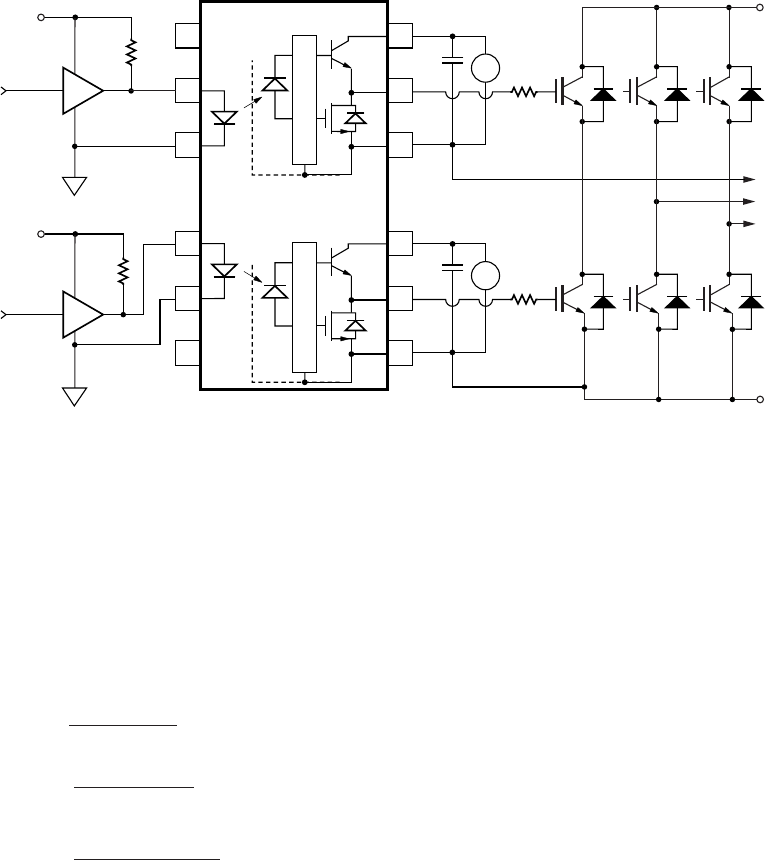
Figure 25b. Recommended LED Drive and Application Circuit (HCPL-315J).
+ HVDC
3-PHASE
AC
0.1 µF
FLOATING
SUPPLY
V
CC
= 18 V
1
3
+
–
2
16
14
15
270 Ω
HCPL-315J
+5 V
CONTROL
INPUT
Rg
74XX
OPEN
COLLECTOR
GND 1
7
6
8
10
11
9
- HVDC
0.1 µF
V
CC
= 18 V
+
–
Rg
270 Ω
+5 V
CONTROL
INPUT
74XX
OPEN
COLLECTOR
GND 1
HCPL-3150 fig 25b