
Datasheet


14
Figure 25a. Recommended LED Drive and Application Circuit.
Applications Information
Eliminating Negative IGBT Gate Drive
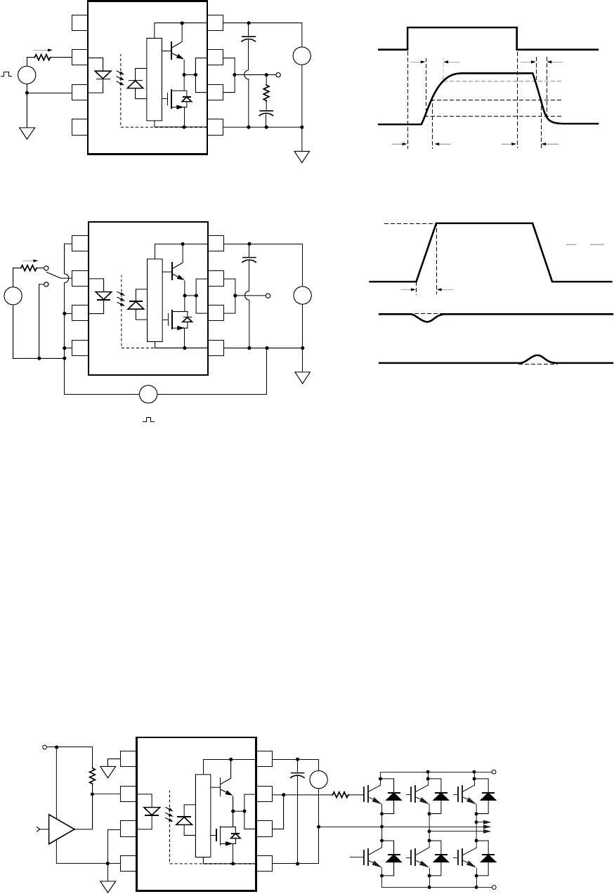
To keep the IGBT rmly o, the HCPL-3150/315J has a
very low maximum V
OL
specication of 1.0 V. The HCPL-
3150/315J realizes this very low V
OL
by using a DMOS
transistor with 4 Ω (typical) on resistance in its pull down
circuit. When the HCPL-3150/315J is in the low state, the
IGBT gate is shorted to the emitter by Rg + 4 Ω. Minimiz-
ing Rg and the lead inductance from the HCPL-3150/315J
to the IGBT gate and emitter (possibly by mounting the
HCPL-3150/315J on a small PC board directly above the
IGBT) can eliminate the need for negative IGBT gate drive
in many applications as shown in Figure 25. Care should
be taken with such a PC board design to avoid routing
the IGBT collector or emitter traces close to the HCPL-
3150/315J input as this can result in unwanted coupling
of transient signals into the HCPL-3150/315J and de-
grade performance. (If the IGBT drain must be routed
near the HCPL-3150/315J input, then the LED should be
reverse-biased when in the o state, to prevent the tran-
sient signals coupled from the IGBT drain from turning
on the HCPL-3150/315J.)
Figure 24. CMR Test Circuit and Waveforms.
HCPL-3150 fig 23
0.1 µF
V
CC
= 15
to 30 V
47 Ω
1
3
I
F
= 7 to 16 mA
V
O
+
–
+
–
2
4
8
6
7
5
10 KHz
50% DUTY
CYCLE
500 Ω
3 nF
I
F
V
OUT
t
PHL
t
PLH
t
f
t
r
10%
50%
90%
Figure 23. t
PLH
, t
PHL
, t
r
, and t
f
Test Circuit and Waveforms.
HCPL-3150 fig 24
0.1 µF
V
CC
= 30 V
1
3
I
F
V
O
+
–
+
–
2
4
8
6
7
5
A
+
–
B
V
CM
= 1500 V
5 V
V
CM
∆t
0 V
V
O
SWITCH AT B: I
F
= 0 mA
V
O
SWITCH AT A: I
F
= 10 mA
V
OL
V
OH
∆t
V
CM
δV
δt
=
+ HVDC
3-PHASE
AC
- HVDC
HCPL-3150 fig 25
0.1 µF
V
CC
= 18 V
1
3
+
–
2
4
8
6
7
5
270 Ω
HCPL-3150
+5 V
CONTROL
INPUT
Rg
Q1
Q2
74XXX
OPEN
COLLECTOR