
Datasheet


14
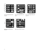
Figure 20. Recommended drive circuit for HCPL-261A/-261N families for high-CMR (similar for HCPL-
263A/-263N).
Application Information
Common-Mode Rejection for HCPL-
261A/HCPL-261N Families:
Figure 20 shows the recommended
drive circuit for the HCPL-261N/-
261A for optimal common-mode
rejection performance. Two main
points to note are:
1. The enable pin is tied to V
CC
rather
than oating (this applies to
single-channel parts only).
2. Two LED-current setting resistors
are used instead of one. This is
to balance I
LED
variation during
common-mode transients.
If the enable pin is left oating, it is
possible for common-mode tran-
sients to couple to the enable pin,
resulting in common-mode failure.
This failure mechanism only occurs
when the LED is on and the output
is in the Low State. It is identied as
occurring when the transient output
voltage rises above 0.8 V. Therefore,
the enable pin should be connected
to either V
CC
or logic-level high for
best common-mode performance
with the output low (CMR
L
). This
failure mechanism is only present
in single-channel parts (HCPL-261N,
-261A, -061N, -061A) which have the
enable function.
Also, common-mode transients can
capacitively couple from the LED an-
ode (or cathode) to the output-side
ground causing current to be shunt-
ed away from the LED (which can be
bad if the LED is on) or conversely
cause current to be injected into the
LED (bad if the LED is meant to be
o). Figure 21 shows the parasitic
capacitances which exists between
LED anode/cathode and output
ground (C
LA
and C
LC
). Also shown in
Figure 21 on the input side is an AC-
equivalent circuit.
*Higher CMR may be obtainable by connecting pins 1, 4 to input ground (Gnd1).
SINGLE CHANNEL PRODUCTS
0.01 µF
350
Ω
HCPL-261A fig 19
74LS04
OR ANY TOTEM-POLE
OUTPUT LOGIC GATE
V
O
V
CC+
8
7
6
1
3
SHIELD
5
2
4
HCPL-261A/261N
GND
GND2
357
Ω
(MAX.)
V
CC
357
Ω
(MAX.)
*
*
* HIGHER CMR MAY BE OBTAINABLE BY CONNECTING PINS 1, 4 TO INPUT GROUND (GND1).
GND1
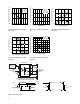
Figure 19. Recommended printed circuit board layout.
DUAL CHANNEL PRODUCTS
ENABLE
(IF USED)
GND BUS (BACK)
V BUS (FRONT)
CC
N.C.
N.C.
N.C.
N.C.
OUTPUT 1
OUTPUT 2
ENABLE
(IF USED)
0.1µF
0.1µF
10 mm MAX. (SEE NOTE 16)
GND BUS (BACK)
V BUS (FRONT)
CC
OUTPUT 1
OUTPUT 2
0.1µF
10 mm MAX. (SEE NOTE 16)