
Datasheet


Dead Time and Propagation Delay Specications
The ACPL-P302/W302 includes a Propagation Delay Dif-
ference (PDD) specication intended to help designers
minimize “dead time” in their power inverter designs. Dead
time is the time high and low side power transistors are o.
Any overlap in Ql and Q2 conduction will result in large
currents owing through the power devices from the high
voltage to the low-voltage motor rails. To minimize dead
time in a given design, the turn on of LED2 should be de-
layed (relative to the turn o of LED1) so that under worst-
case conditions, transistor Q1 has just turned o when
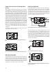
transistor Q2 turns on, as shown in Figure 24. The amount
of delay necessary to achieve this condition is equal to the
maximum value of the propagation delay dierence speci-
cation, PDD max, which is specied to be 500 ns over the
operating temperature range of -40° to 100°C.
Figure 24. Minimum LED Skew for Zero Dead Time.
Figure 25. Waveforms for Dead Time.
Delaying the LED signal by the maximum propagation de-
lay dierence ensures that the minimum dead time is zero,
but it does not tell a designer what the maximum dead
time will be. The maximum dead time is equivalent to the
dierence between the maximum and minimum propaga-
tion delay dierence specication as shown in Figure 25.
The maximum dead time for the ACPL-P302/W302 is 1 µs
(= 0.5 µs - (-0.5 µs)) over the operating temperature range
of –40°C to 100°C.
Note that the propagation delays used to calculate PDD
and dead time are taken at equal temperatures and test
conditions since the optocouplers under consideration are
typically mounted in close proximity to each other and are
switching identical IGBTs.