
Datasheet


11
Applications Information
Eliminating Negative IGBT Gate Drive
To keep the IGBT rmly o, the ACPL-P302/W302 has a
very low maximum V
OL
specication of 1.0 V. Minimizing
R
g
and the lead inductance from the ACPL-P302/W302
to the IGBT gate and emitter (possibly by mounting the
ACPL-P302/W302 on a small PC board directly above the
IGBT) can eliminate the need for negative IGBT gate drive
in many applications as shown in Figure 17. Care should
be taken with such a PC board design to avoid routing
the IGBT collector or emitter traces close to the ACPL-
P302/W302 input as this can result in unwanted coupling
of transient signals into the input of ACPL-P302/W302 and
degrade performance. (If the IGBT drain must be routed
near the ACPL-P302/W302 input, then the LED should be
reverse biased when in the o state, to prevent the tran-
sient signals coupled from the IGBT drain from turning on
the ACPL-P302/W302.
Selecting the Gate Resistor (Rg)
Step 1: Calculate R
g
minimum from the I
OL
peak speci-
cation. The IGBT and R
g
in Figure 17 can be analyzed as
a simple RC circuit with a voltage supplied by the ACPL-
P302/W302.
57.5Ù
0.4
124
I
VV
R
OLPEAK
OLCC
g
=
−
=
−
≥
The V
OL
value of 1 V in the previous equation is the V
OL
at
the peak current of 0.4A. (See Figure 4).
Step 2: Check the ACPL-P302/W302 power dissipation and
increase R
g
if necessary. The ACPL-P302/W302 total power
dissipation (P
T
) is equal to the sum of the emitter power
(P
E
) and the output power (P
O
).
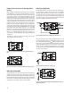
Figure 18. Energy Dissipated in the ACPL-P302/W302 and for Each IGBT Switching
Cycle.
Figure 17. Recommended LED Drive and Application Circuit for ACPL-P302/W302
R
g
270Ω
V
CC
= 15V
+
-
61
52
43
0.1 µF
+5 V
CONTROL
INPUT
74XXX
OPEN
COLLECTOR
+ HVDC
- HVDC
3-PHASE
AC
Q1
Q2
ACPL-P302/W302
+
-
( )
( ) ( )
fQ;REVfQKI
fQ;REVIPPP
DutyCycleVIP
PPP
ggSWCCgICCCCBIAS
ggSWCCCCG)O(SWITCHINO(BIAS)O
FFE
OET
•+•••+=
•+•=+=
••=
+=
where K
ICC
· Q
g
· f is the increase in I
CC
due to switching
and K
ICC
is a constant of 0.001 mA/(nC*kHz). For the circuit
in Figure 17 with I
F
(worst case) = 10 mA, R
g
= 57.5 W, Max
Duty Cycle = 80%, Q
g
= 100 nC, f = 20 kHz and T
AMAX
=
85°C:
( )( )
( )
( )
C@85P250mW126mW20kHz0.3ì.
24V100nC20kHzkHznC0.001mA3mAP
14mW0.81.8V10mAP
MAXO
O
E
°≤=•
+••••+=
=••=
The value of 3 mA for I
CC
in the previous equation is the
max. I
CC
over entire operating temperature range.
Since P
O
for this case is less than P
O(MAX)
, R
g
= 57.5 W is
alright for the power dissipation.