
Data Sheet

AC6368A Datasheet
4
Confidential
The information contained herein is the exclusive property of JIELI and shall not be distributed, reproduced, or disclosed in whole or in part without
prior written permission of JIELI.
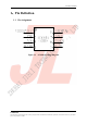
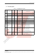
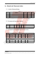
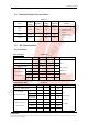
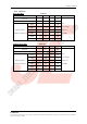
1.2 Pin Description
Table 1-1
AC6368A
Pin Description
PIN
NO.
Name
I/O
Type
Drive
(mA)
Function Other Function
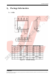
1
VBAT P / Battery Power Supply
VDDIO P / IO Power 3.3v
2 PB1 I/O
GPIO
(pull up)
Long Press Reset
;
ADC5
:
ADC Input Channel 5;
UART0RXB
:
Uart0 Data In(B);
3 VSS P / Ground
4 BT_RF / BT Antenna
5 BTOSCI I BT OSC In
6 BTOSCO O BT OSC Out
7 USBDM I/O
USB Negative
Data
(pull down)
IIC_SDA_A
:
IIC SDA(A);
SPI2_DOB
:
SPI2 Data Out(B);
ADC14
:
ADC Input Channel 14;
UART1RXD
:
Uart1 Data In(D);
8
USBDP I/O
USB Positive
Data
(pull down)
IIC_SCL_A
:
IIC SCL(A);
SPI2_CLKB
:
SPI2 Clock(B);
ADC13
:
ADC Input Channel 13;
UART1TXD
:
Uart1 Data Output(D)
;
PA6 I/O GPIO
ADC4
:
ADC Input Channel 4;
CAP4
:
Timer4 Capture;
UART0RXA
:
Uart0 Data In(A);