
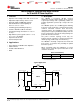
Specifications


LM3269
SNVS793D –NOVEMBER 2011 –REVISED MAY 2015
www.ti.com
System Characteristics (continued)
The following spec table entries are specified by design and verification provided the component values in the typical
application circuit are used (L = 2.2 µH, DCR = 110 mΩ, MIPSZ2520D2R2/FDK; C
IN
= 10 µF, 6.3 V, C1608X5R0J106K/TDK
(0603); C
OUT
= 4.7 µF, 6.3 V, C1608X5R0J475M/TDK (0603). These parameters are not verified by production testing.
Typical (TYP) limits are for T
A
= T
J
= 25°C; minimum (MIN) and maximum (MAX) limits apply over the full operating ambient
temperature range (−30°C ≤ T
J
= T
A
≤ 85°C) and over the V
BATT
= P
VIN
= 2.7 V to 5.5 V, unless otherwise specified.
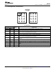
PARAMETER TEST CONDITIONS MIN TYP MAX UNIT
V
BATT
= 3.7 V, V
OUT
= 0.6 V, I
OUT
= 10 mA
61%
−30°C ≤ T
J
= T
A
≤ 85°C
V
BATT
= 3.7 V, V
OUT
= 1 V I
OUT
= 20 mA
78%
−30°C ≤ T
J
= T
A
≤ 85°C
V
BATT
= 3.7 V, V
OUT
= 1.4 V I
OUT
= 50 mA
85%
−30°C ≤ T
J
= T
A
≤ 85°C
η Efficiency
V
BATT
= 3.7 V, V
OUT
= 2.7 V I
OUT
= 200 mA
95%
−30°C ≤ T
J
= T
A
≤ 85°C
V
BATT
= 3.7 V, V
OUT
= 3.3 V, I
OUT
= 480 mA
94%
−30°C ≤ T
J
= T
A
≤ 85°C
V
BATT
= 3 V, V
OUT
= 3.6 V, I
OUT
= 200 mA
95%
−30°C ≤ T
J
= T
A
≤ 85°C
6.7 Switching Characteristics
over operating free-air temperature range (unless otherwise noted)
PARAMETER TEST CONDITIONS MIN TYP MAX UNIT
EN = L to H, V
BATT
= 3.7 V, V
OUT
=
Turnon time (time for output to reach 3.5 V,
T
ON
35 50 µs
0V→90% × 3.5 V) I
OUT
= 0 mA
−30°C ≤ T
J
= T
A
≤ 85°C
V
BATT
= 3.7 V, V
OUT
= 0.6 V, I
OUT
=
F
OSC_PFM
PFM operating frequency 63 kHz
13 mA
F
OSC_PWM
Internal oscillator frequency PWM 2.1 2.4 2.7 MHz
Boost 50%
D
MAX
Maximum duty cycle
Buck 100%
V
BATT
= 3.2 V to 4.7 V,
V
OUT
= 1.4 V to 3 V, 0.1 µs <
V
OUT_TR
VCON change to 90% 10 µs
Tr_
VCON
< 1 µs
R
LOAD
= 11.4 Ω
6 Submit Documentation Feedback Copyright © 2011–2015, Texas Instruments Incorporated
Product Folder Links: LM3269