
Specifications


LM3269
www.ti.com
SNVS793D –NOVEMBER 2011–REVISED MAY 2015
6.5 Electrical Characteristics
Unless otherwise specified, typical (TYP) limits are for T
A
= T
J
= 25°C, and minimum (MIN) and maximum (MAX) limits apply
over the full operating ambient temperature range (−30°C ≤ T
J
= T
A
≤ +85°C). Unless otherwise noted, specifications apply to
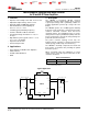
the Figure 16 with: P
VIN
= EN = 3.6V.
(1)(2)
PARAMETER TEST CONDITIONS MIN TYP MAX UNIT
V
FB, min
Min FB voltage VCON = 0.2 V 0.53 0.60 0.67
V
V
FB, max
Max FB voltage VCON = 1.4 V 4.13 4.2 4.27
I
Q_PWM
Quiescent current No switching
(3)
0.9 1.2 mA
EN = 0 V, VCON = 0 V,
I
SHDN
Shutdown supply current 0.02 5 µA
SW1 = SW2 = V
OUT
= 0 V
Open loop
(4)
I
LIM_L
Input current limit (large) 1500 1700 1900
VCON = 1.2 V
mA
Open loop
(4)
I
LIM_S
Input current limit (small) 750 850
VCON = 0.2 V
Gain Internal gain
(5)
0.2 V ≤ VCON ≤ 1.4 V 3 V/V
I
EN
EN pin pulldown current 5 10
µA
I
VCON
VCON pin leakage current –1 1
V
IH
Logic high input threshold for EN 1.2
V
V
IL
Logic low input threshold for EN 0.6
Leakage into VOUT pin of buck- EN = 0 V, V
OUT
≤ 4.2 V
I
OUT_LEAKAGE
5 µA
boost P
VIN
≤ 5.5 V
(1) All voltages are with respect to the potential at the GND pins.
(2) Min and Max limits are specified by design, test, or statistical analysis. Typical numbers are not verified, but do represent the most likely
norm.
(3) I
Q
specified here is when the part is not switching.
(4) The parameters in the electrical characteristics table are tested under open loop conditions at P
VIN
= 3.6 V.
(5) To calculate V
OUT
, use the following equation: V
OUT
= VCON × 3.
6.6 System Characteristics
The following spec table entries are specified by design and verification provided the component values in the typical
application circuit are used (L = 2.2 µH, DCR = 110 mΩ, MIPSZ2520D2R2/FDK; C
IN
= 10 µF, 6.3 V, C1608X5R0J106K/TDK
(0603); C
OUT
= 4.7 µF, 6.3 V, C1608X5R0J475M/TDK (0603). These parameters are not verified by production testing.
Typical (TYP) limits are for T
A
= T
J
= 25°C; minimum (MIN) and maximum (MAX) limits apply over the full operating ambient
temperature range (−30°C ≤ T
J
= T
A
≤ 85°C) and over the V
BATT
= P
VIN
= 2.7 V to 5.5 V, unless otherwise specified.
PARAMETER TEST CONDITIONS MIN TYP MAX UNIT
I
OUT_MAX
Max output current V
BATT
≥ 3 V, V
OUT
= 3.8 V 750 mA
V
CON_LIN
VCON linearity 0.2 V ≤ VCON ≤ 1.4 V –2.5% 2.5%
V
BATT
≥ 3.2 V, 0.6 V ≤ V
OUT
≤ 4.2 V,
Ripple voltage 15 50
0 mA ≤ I
OUT
≤ 430 mA, T
A
= 25°C
PFM ripple V
OUT
= 0.6 V, I
OUT
= 5 mA 45
V
O_RIPPLE
mV
V
BATT
= 3 V to 5 V,
Ripple voltage in mode
T
R
= T
F
= 30 µs 50
transition
3.3 V ≤ V
OUT
≤ 4.2 V
V
BATT
= 2.7 V to 4.7 V, V
OUT
= 3.8 V,
Line regulation 10
I
OUT
= 500 mA
ΔV
OUT
mV
Load regulation I
OUT
= 0 mA to 500 mA, V
BATT
= 2.7 V to 4.7 V 20
V
BATT
= 3.2 V to 4.7 V,
V
OUT_TR
VOUT rise time V
OUT
= 1.4 V to 3 V, 0.1 µs < Tr_
VCON
< 1 µs 10 µs
R
LOAD
= 11.4 Ω
Copyright © 2011–2015, Texas Instruments Incorporated Submit Documentation Feedback 5
Product Folder Links: LM3269