
Specifications


LM3269
SNVS793D –NOVEMBER 2011 –REVISED MAY 2015
www.ti.com
6 Specifications
6.1 Absolute Maximum Ratings
over operating free-air temperature range (unless otherwise noted)
(1)(2)
MIN MAX UNIT
PVIN, VOUT to GND −0.2 6 V
EN, VCON to SGND, PGND −0.2 P
VIN
+ 0.2 V or 6 V
(3)
V
FB to PGND −0.2 V
OUT
+ 0.2 V or 6 V
(3)
V
SW1, SW2 −0.2 P
VIN
+ 0.2 V or 6 V
(3)
V
Continuous power dissipation
(4)
Internally limited
Junction temperature, T
J-MAX
150 °C
Storage temperature, T
stg
−65 150 °C
(1) Stresses beyond those listed under Absolute Maximum Ratings may cause permanent damage to the device. These are stress ratings
only, which do not imply functional operation of the device at these or any other conditions beyond those indicated under Recommended
Operating Conditions. Exposure to absolute-maximum-rated conditions for extended periods may affect device reliability.
(2) If Military/Aerospace specified devices are required, please contact the Texas Instruments Sales Office/Distributors for availability and
specifications.
(3) Whichever is smaller.
(4) Internal thermal circuitry protects the device from permanent damage. Thermal shutdown engages at T
J
= 150°C (typical) and
disengages at T
J
= 125°C (typical).
6.2 ESD Ratings
VALUE UNIT
V
(ESD)
Electrostatic discharge Human-body model (HBM), per ANSI/ESDA/JEDEC JS-001
(1)
±2000 V
(1) JEDEC document JEP155 states that 500-V HBM allows safe manufacturing with a standard ESD control process.
6.3 Recommended Operating Conditions
over operating free-air temperature range (unless otherwise noted)
(1)(2)
MIN NOM MAX UNIT
Input voltage 2.7 5.5 V
Output voltage 0.6 4.2 V
Recommended load current 0 750 mA
Junction temperature (T
J
) −30 125 °C
Ambient temperature (T
A
)
(3)
−30 85 °C
(1) Stresses beyond those listed under absolute maximum ratings may cause permanent damage to the device. These are stress ratings
only, and functional operation of the device at these or any other conditions beyond those indicated under recommended operating
conditions is not implied. Exposure to absolute-maximum-rated conditions for extended periods may affect device reliability.
(2) All voltages are with respect to the potential at the GND pins.
(3) In applications where high power dissipation and/or poor package thermal resistance is present, the maximum ambient temperature may
have to be de-rated. Maximum ambient temperature (T
A-MAX
) is dependent on the maximum operating junction temperature (T
J-MAX-OP
=
125°C), the maximum power dissipation of the device in the application (P
D-MAX
), and the junction-to ambient thermal resistance of the
part/package in the application (R
θJA
), as given by the following equation: T
A-MAX
= T
J-MAX-OP
– (R
θJA
× P
D-MAX
).
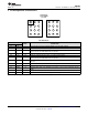
6.4 Thermal Information
LM3269
THERMAL METRIC
(1)
YZR (DSBGA) UNIT
12 PINS
R
θJA
Junction-to-ambient thermal resistance
(2)
85 °C/W
(1) For more information about traditional and new thermal metrics, see the IC Package Thermal Metrics application report, SPRA953.
(2) Junction-to-ambient thermal resistance is highly application and board-layout dependent. In applications where high maximum power
dissipation exists, special care must be paid to thermal dissipation issues in board design. Junction-to-ambient thermal resistance (R
θJA
)
is taken from a thermal modeling result, performed under the conditions and guidelines set forth in the JEDEC standard JESD51-7.
4 Submit Documentation Feedback Copyright © 2011–2015, Texas Instruments Incorporated
Product Folder Links: LM3269