
Specifications
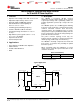


Top View Bottom View
A1A2A3
D1D2
B1B2B3
C1C2C3
D3
A1 A2 A3
D1 D2 D3
B1 B2 B3
C1 C2 C3
LM3269
www.ti.com
SNVS793D –NOVEMBER 2011–REVISED MAY 2015
5 Pin Configuration and Functions
YZR Package
12-Pin DSBGA
Top View
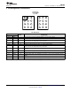
Pin Functions
PIN
TYPE
(1)
DESCRIPTION
NUMBER NAME
A1 NC — Non Connection. Leave this pin floating; do not connect to PVIN or PGND.
A2 NC — Non Connection. Leave this pin floating, do not connect to PVIN or PGND.
A3 PVIN P/I Power MOSFET input and power current input pin. Optional low-pass filtering may help buck and
buck-boost modes for radiated EMI and noise reduction.
B1 VCON A/I Voltage Control analog input. VCON controls the output voltage in PWM and PFM modes.
B2 EN D/I Enable pin. Pulling this pin higher than 1.2 V enables part to function.
B3 PVIN P/I Power MOSFET input and power current input pin. Optional low-pass filtering may help buck and
buck-boost modes for radiated EMI and noise reduction.
C1 FB A Feedback input to inverting input of error amplifier. Connect output voltage directly to this node at
load point.
C2 SGND G Signal Ground for analog circuits and control circuitry.
C3 SW1 P/O Switch pin for Internal Power Switches. Connect inductor between SW1 and SW2.
D1 VOUT O Regulated output voltage of the LM3269. Connect this to a 4.7-µF ceramic output filter capacitor
to GND.
D2 SW2 P/O Switch pin for Internal Power Switches. Connect inductor between SW1 and SW2.
D3 PGND G Power Ground for Power MOSFETs and gate drive circuitry.
(1) A: Analog Pin, D: Digital Pin, G: Ground Pin, P: Power Pin, I: Input Pin, O: Output Pin.
Copyright © 2011–2015, Texas Instruments Incorporated Submit Documentation Feedback 3
Product Folder Links: LM3269