
Specifications


FB
NC
VCON VOUT
EN SGND SW2
PVIN PVIN
SW1 PGND
NC
C4
C1
C2
C3
L2
LM3269
L1
LM3269
www.ti.com
SNVS793D –NOVEMBER 2011–REVISED MAY 2015
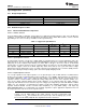
10.1.1.4 Component Placement
Figure 17. LM3269 Recommended Parts Placement (Top View)
10.1.1.5 PCB Considerations By Layer
10.1.1.5.1 VBATT
Use a star connection from VBATT to LM3269 and VBATT to PA VBATT (VCC1) connection. Do not daisy-chain
VBATT connection to LM3269 circuit and then to PA device VBATT connection.
Top Layer (Numbers correspond to those in the Layout Examples section.)
1. Create a PGND island as shown. PGND pads of C2 (CIN) and C3 (COUT) must be isolated from each other.
This PGND island will connect to the dedicated system ground with many vias.
2. Each SW (C3) and (D2) bump will have a via in pad and an additional via next to it, to drop down the SW
trace to layer
3. SGND bump (C2) will have a via in pad, and directly connecting it to the system ground.
4. FB (C1) should connect directly to the VOUT bump (D1).
5. Have PVIN vias next to optional ferrite bead.
6. Leave NC bumps (A1 and A2) floating; Do not connect to VBATT or GND
Layer 2
7. VCON and Digital logic signals may be routed on this layer.
8. VOUT (VCC2 of PA) can be routed on this layer.
9. PVIN for the LM3269 can be routed on this layer.
Layer 3
10. Each SW trace is routed on this layer. The width of each trace should be 15 mils (0.381 mm) for current
capabilities. Have two vias bring each SW trace up to the inductor pads.
Layer 4
11. Connect the PGND, SGND, and high Frequency vias from the top layer on this layer.
Copyright © 2011–2015, Texas Instruments Incorporated Submit Documentation Feedback 17
Product Folder Links: LM3269