
Specifications


LM3269
SNVS793D –NOVEMBER 2011 –REVISED MAY 2015
www.ti.com
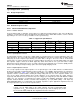
P
VIN
Step = 3.6 V V
OUT
= 3 V Load = 320 mA
P
VIN
= 3.6 V V
OUT
= 3.45 V Load = 350 mA
↔ 4.2 V
Figure 13. Start-Up
Figure 14. Line Transient For DC-DC
P
VIN
= 3.8 V V
OUT
= 3.45 V
Figure 15. Load Transient DC-DC
9 Power Supply Recommendations
The LM3269 device is designed to operate from an input voltage supply range between 2.7 V and 5.5 V. This
input supply should be well regulated. If the input supply is located more than a few inches from the LM3269
converter additional bulk capacitance may be required in addition to the ceramic bypass capacitors. An
electrolytic or tantalum capacitor with a value of 47 μF is a typical choice.
14 Submit Documentation Feedback Copyright © 2011–2015, Texas Instruments Incorporated
Product Folder Links: LM3269