
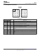
Specifications


LM3269
SNVS793D –NOVEMBER 2011 –REVISED MAY 2015
www.ti.com
7.3 Feature Description
7.3.1 Dynamically Adjustable Output Voltage
The LM3269 features a dynamically adjustable output voltage to eliminate the need for external feedback
resistors. The output can be set from 0.6 V to 4.2 V by changing the voltage on the analog VCON pin. This
feature is useful in cell phone RF PA applications where peak power is needed only when the handset is far
away from the base station or when data is being transmitted. In other instances, the transmitting power can be
reduced; therefore the supply voltage to the PA can be reduced, promoting longer battery life. In order to
adaptively adjust the supply voltage to the PA in real time in a cell-phone application, the output voltage
transition should be fast enough to meet the RF transmit signal specifications. The LM3269 offers ultra-fast
output voltage transition without drawing very large currents from the battery supply. For a current limit of 1700
mA (typical), the output voltage can transition from 1.4 V to 3 V in 10 µs with a load resistance of 11.4 Ω.
7.3.2 Seamless Buck Transition
The LM3269 features a unique internal power switch topology that improves converter efficiency, especially
compared to typical non-inverting buck-boost converters. The LM3269 operates either as buck converter or a
boost converter, depending upon the input and output voltage conditions. This creates a boundary between the
buck and boost mode of operation. When the input battery voltage is close to the set output voltage, the
converter automatically switches seamlessly such that the output voltage does not see any perturbations at the
mode boundary. The excellent mode transition capability of the LM3269 enables low noise output with highest
efficiency. Internal feedback loop compensation ensures stable operation in buck, boost and buck-boost mode
transition operation.
7.3.3 Thermal Overload Protection
The LM3269 has a thermal overload protection function that operates to protect itself from short-term misuse and
over-load conditions. When the junction temperature exceeds around 150°C, the device inhibits operation. All
power MOSFET switches are turned off in PWM mode. When the temperature drops below 125°C, normal
operation resumes. Prolonged operation in thermal overload conditions may damage the device and is
considered bad practice.
7.4 Device Functional Modes
7.4.1 Enable And Shutdown Mode
Setting the EN digital pin low (< 0.6 V) places the LM3269 in shutdown mode (0.01 μA typical). During shutdown,
the output of the LM3269 is tri-stated, maintaining charge storage on the output capacitor. Setting EN high ( > 1.2
V) enables normal operation. EN should be set low to turn off the LM3269 during power up and undervoltage
conditions when the power supply (PVIN) is less than the 2.7-V minimum operating voltage.
7.4.2 V
CON,ON
The output is disabled when VCON is below 125 mV (typical). It is enabled when VCON is above 150 mV
(typical). The threshold has approximately 25 mV (typical) of hysteresis.
7.4.3 Pulse Frequency Modulation (PFM) Mode
The LM3269 enters PFM mode and operates with reduced switching frequency and supply current to maintain
very high efficiencies when the output voltage is less than 1.5 V. In PFM mode, the LM3269 will support up to
120 mA max. In PFM, if the output voltage exceeds 1.5 V, the device will automatically transition into a forced
PWM mode of operation.
10 Submit Documentation Feedback Copyright © 2011–2015, Texas Instruments Incorporated
Product Folder Links: LM3269