
Data Sheet

TSYS01 Digital Temperature Sensor
TSYS01 Rev 11 www.meas-spec.com 2013-03
5/10
INTERFACE DESCRIPTION
PROTOCOL SELECTION
PS pin input level has to be defined in dependence to protocol selection.
PS = 0 activates SPI.
PS = 1 activates I
2
C.
I
2
C INTERFACE
A I
2
C communication message starts with a start condition and it is ended by a stop condition.
Each command consists of two bytes: the address byte and command byte.
I
2
C ADDRESS SELECTION
The I
2
C address can be selected by CSB pin.
CSB=1 then the address is 1110110x.
CSB=0 the address is 1110111x.
Therefore, two TSYS01 can be interfaced on the same I
2
C bus.
SPI INTERFACE
The serial interface is a 4-wire SPI bus, operating as a slave. CS (chip select), SCLK (serial clock), SDI
(serial data in), and SDO (serial data out) are used to interact with the SPI master.
Communication with the chip starts when CS is pulled to low and ends when CS is pulled to high.
SCLK is controlled by the SPI master and idles low (SCLK low on CS transitions, mode 0).
A mode where the clock alternatively idles high is also supported (mode 3).
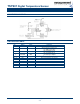
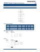
COMMANDS
The commands are the same for SPI and I
2
C interface.
There are four commands:
Reset
Read PROM (calibration parameters)
Start ADC Temperature conversion
Read ADC Temperature result
Command
Hex Value
Reset
0x1E
Start ADC Temperature Conversion
0x48
Read ADC Temperature Result
0x00
PROM Read Address 0
0xA0
PROM Read Address 1
0xA2
PROM Read Address 2
0xA4
PROM Read Address 3
0xA6
PROM Read Address 4
0xA8
PROM Read Address 5
0xAA
PROM Read Address 6
0xAC
PROM Read Address 7
0xAE