
Service manual


Samsung Electronics 2-1
2. Reference Information
2-1 IC Dsecriptions
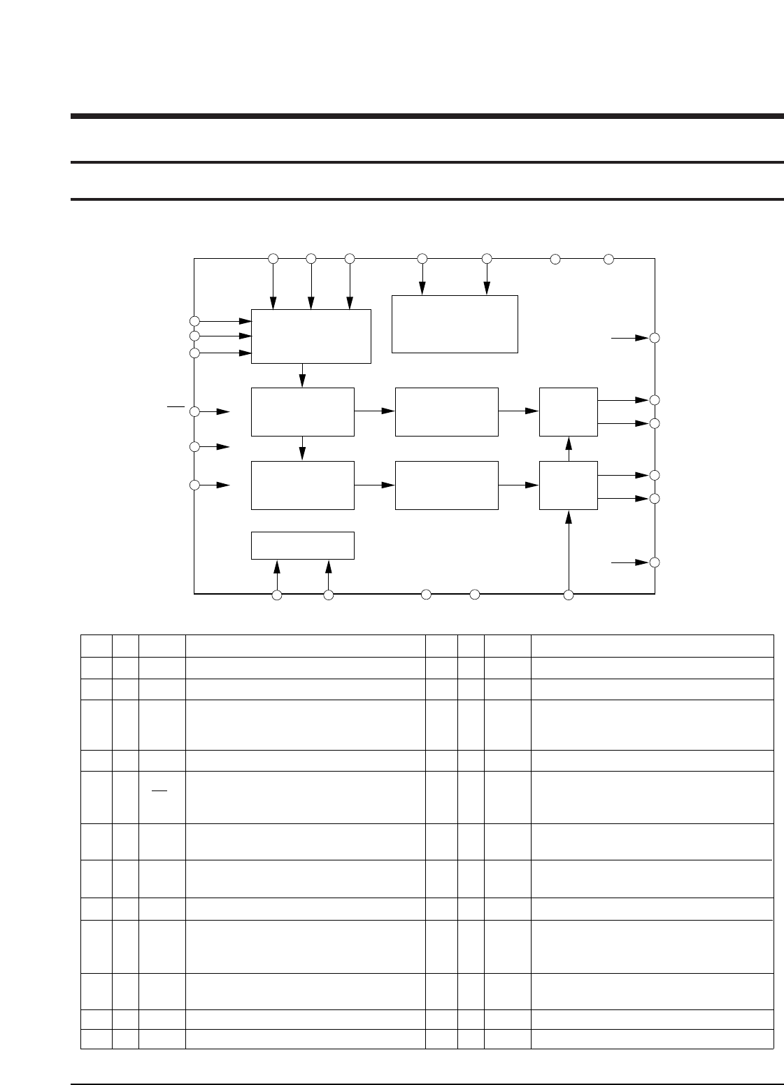
2-1-1 AIC1 (AK4324 ; Digital-to-Analog Converter)
Serial Input
Interface
De-emphasis
Control
8X
Interpolator
8X
Interpolator
∆ ∑
Modulator
SCF
SCF
∆ ∑
Modulator
Clock Divider
DIF0 DIF1 DIF2 DEM0 DEM1 AVDD AVSS
VREFDVSSDVDDCKSMCLK
LRCK
BICK
SDATA
SMUTE
DFS
DZFL
AOUTL+
AOUTL-
AOUTR+
AOUTR-
DZFR
PD
NAME
DVSS
DVDD
CKS
MCLK
BICK
SDATA
PD
I/O
I
I
I
I
I
PIN
1
2
3
4
5
6
I
7
LRCK
I
8
FUNCTION
NAME
I/O
PIN
FUNCTION
Digital ground pin
Digital power supply
Master clock select pin (Internal pull-down pin)
Nomal speed "L":MCLK = 256fs, "H":MCLK = 384fs
Double speed "L":MCLK = 128fs, "H":MCLK = 192fs
Master clock input pin
Power-Down mode pin. When at "L", the AK4324 is in
power-down and is held in rest.
The AK4324 should always be reset upon power-pin
I SMUTE
9
I DFS
10
I DEM0
11
Soft mute pin
When this pin goes "H", soft mute cycle is initiated
When returning "L", the output mute releases.
Audio serial data input pin
64fs clock is recommended to be input on this pin
Audio serial data input pin
2's complement MSB-first data is input on this pin.
Double speed sampling mode pin (Internal pull-down pin)
"L":normal speed, "H":double speed
L/R clock pin.
De-emphasis frequency select pin
I DEM1
12
De-emphasis frequency select pin
Note : Allinput pins except internal pull-down pins should not be left floating.
-
DZFL
O
Lch positive analog output pin
Analog ground pin
Voltage reference input pin
Analog power supply pin.
Rch zero input detect pin
Lch zero input detect pin
I DIF0
13
Digital input format pin
I DIF1
14
Digital input format pin
I DIF2
15
Digital input format pin
0 AOUTR-
16
Rch negative analog output pin
O AOUTR+
17
Rch positive analog output pin
O AOUTL-
AOUTL+
18
O
19
AVSS
-
20
VREF
O
21
AVDD
O
22
DZFR
O
23
24
Lch negative analog output pin