User's Manual
Table Of Contents
- Installation and Operation Manual
- Table of Contents
- Introduction
- Installation
- Cautionary Notes
- Pre-RF Connection Tests
- OPERATION
- Signal flow
- System Components
- Field Adjustments
- Maintenance and Repair
- Recommended replacement parts
- Conversion Chart

61-38-05 UserMan page 18 of 38
TXRX Systems Inc. Manual 7-9408-1.2 07/25/05 Page 18
larger. This change causes the output of IC2 to
also become increasingly negative. This output
voltage is connected via diode D1 to bias the PIN
diode attenuator. As this voltage becomes more
negative, the attenuation is increased thus achiev-
ing a certain range of gain control. Diode D1
insures that the gain control voltage is always posi-
tive and never goes below 0 volts. In actual opera-
tion, OLC operation is set to commence when the
power output of the final amplifier reaches its maxi-
mum two-carrier level as shown on the specifica-
tion drawing.
Two other IC’s are mounted on the DC control cir-
cuit board. IC1 is a 10 volt regulator that supplies
DC to the other two chips. Variable resistor VR1 is
used to set this voltage. IC3 is a voltage inverter
that produces -4.5 volts which is applied to the op-
amp IC2. This negative bias allows the output volt-
age of IC2 to closely approach 0 volts.
The PIN diode attenuator board has two diodes
that are used in series to extend the attenuation
range. The diodes are always forward biased with
minimum forward resistance and insertion loss
occurring at about 20 ma of current.
Pre-Amplifier Stage (3-11423)
The pre-amplifier consists of the 400 milliwatt
amplifier stage connected to the input of the OLC
assembly. The preamp is the first stage of the four
identical stages found in the amplifier assembly 3-
11423. This amplifier stage is used to insure that a
sufficient signal level is applied to the OLC assem-
bly.
The 1-section/3-section amplifier assembly (3-
11423) is composed of four individual and identical
amplifier sections. Each of the individual sections
(part# 3-8089) are complete 400 milliwatt amplifi-
ers. The individual sections are mounted on a com-
mon mounting panel and have a common DC
distribution bus running internally between them.
Each section provides 18.5 dB of gain with a power
requirement of 21.7 VDC (nominal) and a typical
current draw of 121 ma. The maximum single car-
rier power output is 400 milliwatts.
Each 400 milliwatt amplifier section consists of two
circuits, the amplifier circuit (3-8087) and the bias
regulator circuit (3-10742). Both of these circuits
are housed in their own enclosures which are then
physically joined together to make up one section.
The circuits are electrically joined using feed-thru
capacitors Cf1 and Cf2.
The amplifier circuit uses a linear RF transistor Q1
(Phillips part# BFQ34/01) which is operated in a
class "A" configuration in order to keep any inter-
modulation distortion to a minimum. The RF tran-
sistor is biased for a nominal collector current of
121 ma. A bias regulator circuit is used to keep the
collector current constant with changes in tempera-
ture. Narrow band matching techniques are used in
this amplifier and it will require tuning if the transis-
tor or matching network components are replaced.
CONTROL
VOLTAGE
+15 VDC
OUTPUT
INPUT
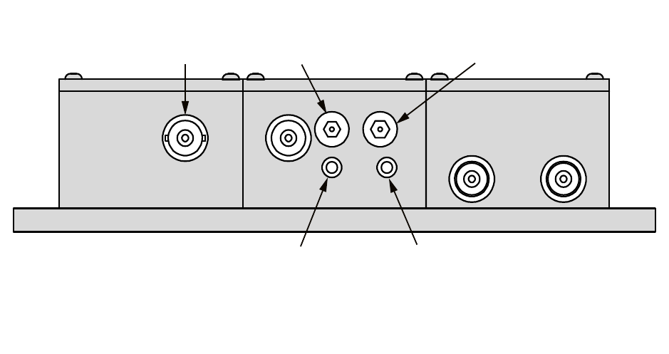
OLC Voltage
Adjust
10V Regulator
Adjust
RF from
Sampler
Detector
Voltage
Test Point
OLC
Voltage
Test Point
RF to DC
Converter
Pin Diode
Attenuator
Figure 8
: OLC assembly 3-6280.


