User's Manual
Table Of Contents
- Installation and Operation Manual
- Table of Contents
- Introduction
- Installation
- Cautionary Notes
- Pre-RF Connection Tests
- OPERATION
- Signal flow
- System Components
- Field Adjustments
- Maintenance and Repair
- Recommended replacement parts
- Conversion Chart

TXRX Systems Inc. Manual 7-9408-1.2 07/25/05 Page 15
61-38-05 UserMan page 15 of 38
-50 dB coupling loss of the signal sampler and any
additional loss produced by attenuator pads on the
analyzer input. A pad on the analyzer input can
help to minimize measurement errors due to
VSWR mismatch that occurs with some analyzers.
A pair of fixed attenuator pads (3 and 6 dB) are
supplied for the purpose of gain reduction. They
are mounted in clips to the top of the filter assem-
blies in the center of the unit. The pads’ attenuation
values are clearly labeled on the body of the atten-
uator. The correct position for adding fixed pads to
the system is at the input or output of the electronic
attenuator ports on the OLC assembly (shown as
the dotted outline symbols on the specification
drawing).
CAUTION
: Any fixed attenuator pads
that are already connected into the
booster circuitry have been installed
at the factory and should not be
removed for any reason. Their func-
tion may be other than gain reduc-
tion.
BYPASSING AMPLIFIER SECTIONS
Sometimes the amount of gain reduction needed is
greater than the amount available with the fixed
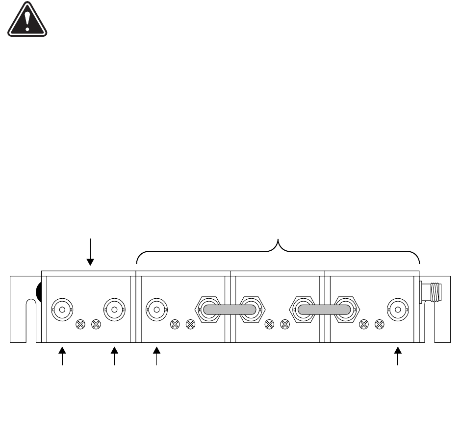
attenuator pads alone. In this case, the first stage
of the three stage portion of amplifier assembly (3-
11423) in the uplink or downlink branch may be
bypassed. The individual stages of these multi-
stage amplifiers are connected together with short
lengths of coaxial cable. To bypass the first stage of
the driver amp remove the coax cable that inter-
connects the first and second stages of the driver
amplifier (see
Figure 7
). Move the input cable from
the input connector on the first stage to the corre-
sponding connector on the second stage of the
driver amp. The BNC RF input connector for each
amplifier stage is located furthest from the DC
input TNC connector. Keep in mind that the total
gain reduction is the sum of the added padding
plus the loss of gain for the bypassed amplifier sec-
tion. Quality 50 ohm terminations should be
installed on the open terminals of any bypassed
stage.
OPERATION
It is imperative that the pre-installation checks be
performed as outlined earlier. Failure to do so may
lead to unsatisfactory operation or damage to the
signal booster. All that is required in order to put
the system into operation after the installation is to
turn on the power supply assembly. The green LED
on the power supply will illuminate indicating nor-
mal operation. If the red LED on the power supply
assembly illuminates it indicates operation from the
backup power source.
SIGNAL FLOW
Signal flow through the system is illustrated using
the system block diagram that is shown in specifi-
cations drawing shipped with your system. The 61-
38-05 model signal boosters are composed of 2
branches, uplink and downlink. Because the uplink
Pre-Amp
(Single Stage)
Driver Amp
(3 Cascaded Stages)
RF
Output
RF
Input
RF
Output
RF
Input
Figure 7:
1stg/3stg amplifier assembly 3-11423.


