EXHIBIT 2 PAGE 1 OF 17 Part No. 7-9257-1 Installation and Setup Manual for the One-way Signal Booster System Model Number 60-96-00400-G1 Copyright (c) 2000 TX Rx Systems, Inc. First Printing: November 2000 TX RX Systems Inc.
EXHIBIT 2 PAGE 2 OF 17 WARRANTY This warranty applies for one year from shipping date. TX RX SYSTEMS INC. warrants its products to be free from defects in material and workmanship at the time of shipment. Our obligation under warranty is limited to replacement or repair at our option, of any such products (with the exception of tubes) which shall have been defective at the time of manufacture. TX RX SYSTEMS INC.
EXHIBIT 2 PAGE 3 OF 17 Table of Contents General Description Note About Output Power Rating Installation Cautionary Note Pre-RF Connection Tests Test Equipment Antenna Isolation Procedure for Measuring Antenna Isolation Increasing Isolation Input Signal Levels Procedure for Measuring Input Signal Levels Reduction of Incoming Signal Strength Setting Signal Booster Gain Gain Reduction Methods Bypassing Amplifier Stages Operation Performance Survey Maintenance and Repair Detailed Subassembly Descriptions Pres
EXHIBIT 2 PAGE 4 OF 17 GENERAL DESCRIPTION Signal boosters extend radio coverage into areas where abrupt propagation losses prevent reliable communication. This system receives an RF signal, raises its power level, and couples it to an antenna or leaky (radiating) coaxial cable system so that it can be re-radiated. No frequency translation (conversion) occurs with this device.
EXHIBIT 2 PAGE 5 OF 17 same amount but will come out at power levels that are related to their respective input level by the gain specification. Signal leveling is not an intended function of a signal booster. Amplifier stages used in this signal booster system may be damaged by excessively strong input signal levels. The system is equipped with Output Leveling Circuitry (OLC) to protect the amplifiers and reduce spurious signals.
EXHIBIT 2 PAGE 6 OF 17 of and help you to avoid the areas where experience has shown us that trouble can occur. 1) Just like the feedback squeal that can occur when the microphone and speaker get too close to each other in a public address system, a signal booster can start to self oscillate. This will occur when the isolation between the input antenna or signal source and the output distribution system does not exceed the signal boosters gain by at least 15 dB.
EXHIBIT 2 PAGE 7 OF 17 Antenna Isolation Antenna isolation is the signal path isolation between the two sections of the signal distribution system that are to be connected to the signal boosters antenna ports. Lack of isolation between the input and output antennas can cause the amplifiers in the system to oscillate. This can happen at a high enough level to damage the power amplifier stages.
EXHIBIT 2 PAGE 8 OF 17 can also occur giving weaker signals than desired. e) Signal booster model with excessive gain. In systems that have an existing signal booster, it is sometimes assumed that an identical unit should be installed when expanding the system to provide extended coverage. In most cases, a signal booster with far less gain than the first is required. f) Improper installation or application of signal splitters or directional couplers in the signal distribution system.
EXHIBIT 2 PAGE 9 OF 17 First we use the conversion chart at the end of this manual to convert the power levels in dBm to watts so that we can add them together. The power in watts is written in scientific notation but the chart uses computer notation. For example, in the chart, an exponent may be written as E-08. In conventional mathematical notation E-08 is written 10-8. The total power must be written as a number between 0 and 10 to use the chart. Look up 1.611E-7 in the Watts column.
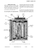
EXHIBIT 2 PAGE 10 OF 17 put amp (part of the OLC assembly). This port is for the connection of test equipment such as a spectrum analyzer and will allow the observation of the amplifier output at a considerably reduced output level. This decoupling figure needs to be added to a measured signal value in order to arrive at the actual signal level. power supply assembly is functioning normally. The red LED is not used.
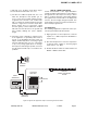
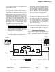
EXHIBIT 2 PAGE 11 OF 17 SPECTRUM ANALYZER SIGNAL DISTRIBUTION SYSTEM BOOSTED RF SIGNAL 10 dB Pad OLC Assembly DC Control Detector Filter Filter Amp Sampler Electronic Attenuator Sampler DC Figure 5: Test equipment interconnection for surveying performance. are subjected to excessively high signal levels, power surges or lightning strikes, failures may occur. The following procedures may be followed for detecting a malfunctioning unit or as part of a periodic maintenance program.
EXHIBIT 2 PAGE 12 OF 17 bands. The combline output filters suppress any IM products that may be inadvertently generated. handle short term or transient overdrive episodes only. OLC Assembly 3-9417 This circuitry actuates when the predetermined maximum output level is reached. The output power level is sensed with a signal sampler that is built into the OLC assembly. The sampler outputs to a detector circuit which generates a DC voltage that is proportional to the output power level.
EXHIBIT 2 PAGE 13 OF 17 supplied to a "TNC" female connector to power this assembly. The RF to DC converter section of the OLC assembly contains three circuits, a -20 dB sampler which is used to supply the RF signal to the diode detector, and finally a -50 dB sampler which provides a convenience port for connecting test equipment. The detector circuit receives RF from the -20 dB sampler and produces a negative polarity DC output voltage that is proportional to the RF signal.
EXHIBIT 2 PAGE 14 OF 17 Repair or replacement of bias circuit components does not necessitate retuning of the amplifier. components does not necessitate retuning of the amplifier. First Driver Amplifier 3-11432 The remaining four stages of the five stage assembly (3-11432) are used to form a driver amplifier which amplifies the output of the OLC assembly and applies it to the second driver amp. Power Amplifier 3-3948 This 6 watt final amplifier uses a single ultra-linear RF transistor.
EXHIBIT 2 PAGE 15 OF 17 Power Conversion Chart dBm to dBw : Watts : Microvolts dBm dBw Watts Volts (50Ω) dBm dBw Watts Volts (50Ω) 80 50 100000 2236.07 40 10 10 22.36 79 49 79432.82 1992.9 39 9 7.94 19.93 78 48 63095.74 1776.17 38 8 6.31 17.76 77 47 50118.72 1583.01 37 7 5.01 15.83 76 46 39810.72 1410.86 36 6 3.98 14.11 75 45 31622.78 1257.43 35 5 3.16 12.57 74 44 25118.86 1120.69 34 4 2.51 11.21 73 43 19952.62 998.81 33 3 2 9.
EXHIBIT 2 PAGE 16 OF 17 Power Conversion Chart dBm to dBw : Watts : Microvolts dBm dBw Watts uVolts (50Ω) dBm dBw Watts uVolts (50Ω) 0 -30 1.0000E-03 223606.8 -40 -70 1.0000E-07 2236.07 -1 -31 7.9433E-04 199289.77 -41 -71 7.9433E-08 1992.9 -2 -32 6.3096E-04 177617.19 -42 -72 6.3096E-08 1776.17 -3 -33 5.0119E-04 158301.49 -43 -73 5.0119E-08 1583.02 -4 -34 3.9811E-04 141086.35 -44 -74 3.9811E-08 1410.86 -5 -35 3.1623E-04 125743.34 -45 -75 3.
EXHIBIT 2 PAGE 17 OF 17 Power Conversion Chart dBm to dBw : Watts : Microvolts dBm dBw Watts uVolts (50Ω) dBm -80 -110 1.0000E-11 22.36 -120 -81 -111 7.9433E-12 19.93 -121 -82 -112 6.3096E-12 17.76 -122 -83 -113 5.0119E-12 15.83 -84 -114 3.9811E-12 -85 -115 -86 -116 -87 dBw Watts uVolts (50Ω) -150 1.0000E-15 0.22 -151 7.9433E-16 0.2 -152 6.3096E-16 0.18 -123 -153 5.0119E-16 0.16 14.11 -124 -154 3.9811E-16 0.14 3.1623E-12 12.57 -125 -155 3.