
Datasheet


ST72334J/N, ST72314J/N, ST72124J
136/153
COMMUNICATION INTERFACE CHARACTERISTICS (Cont’d)
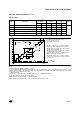
Figure 96. SPI Slave Timing Diagram with CPHA=1
1)
Figure 97. SPI Master Timing Diagram
1)
Notes:
1. Measurement points are done at CMOS levels: 0.3xV
DD
and 0.7xV
DD
.
2. When no communication is on-going the data output line of the SPI (MOSI in master mode, MISO in slave mode) has
its alternate function capability released. In this case, the pin status depends of the I/O port configuration.
SS
INPUT
SCK
INPUT
CPHA=0
MOSI
INPUT
MISO
OUTPUT
CPHA=0
t
w(SCKH)
t
w(SCKL)
t
r(SCK)
t
f(SCK)
t
a(SO)
t
su(SI)
t
h(SI)
MSB OUT BIT6 OUT
LSB OUT
see
CPOL=0
CPOL=1
t
su(SS)
t
h(SS)
t
dis(SO)
t
h(SO)
see
note 2note 2
t
c(SCK)
HZ
t
v(SO)
MSB IN
LSB IN
BIT1 IN
SS
INPUT
SCK
INPUT
CPHA=0
MOSI
OUTPUT
MISO
INPUT
CPHA=0
CPHA=1
CPHA=1
t
c(SCK)
t
w(SCKH)
t
w(SCKL)
t
h(MI)
t
su(MI)
t
v(MO)
t
h(MO)
MSB IN
MSB OUT
BIT6 IN
BIT6 OUT
LSB OUT
LSB IN
see note 2 seenote2
CPOL=0
CPOL=1
CPOL=0
CPOL=1
t
r(SCK)
t
f(SCK)