
User Manual


element14 is a trademark of Premier Farnell plc 93
© 2014 Premier Farnell plc. All Rights Reserved
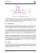
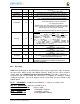
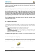
Figure 61 Expansion Board EEPROM Without Write Protect
The addressing of this device requires two bytes for the address which is not used on
smaller size EEPROMs, which only require only one byte. Other compatible devices may
be used as well. Make sure the device you select supports 16 bit addressing. The part
package used is at the discretion of the cape designer.
8.2.1 EEPROM Address
In order for each cape to have a unique address, a board ID scheme is used that sets the
address to be different depending on the setting of the dipswitch or jumpers on the capes.
A two position dipswitch or jumpers is used to set the address pins of the EEPROM.
It is the responsibility of the user to set the proper address for each board and the position
in the stack that the board occupies has nothing to do with which board gets first choice
on the usage of the expansion bus signals. The process for making that determination and
resolving conflicts is left up to the SW and, as of this moment in time, this method is a
something of a mystery due t the new Device Tree methodology introduced in the 3.8
kernel.
Address line A2 is always tied high. This sets the allowable address range for the
expansion cards to
0x54
to
0x57
. All other I2C addresses can be used by the user in the
design of their capes. But, these addresses must not be used other than for the board
EEPROM information. This also allows for the inclusion of EEPROM devices on the
cape if needed without interfering with this EEPROM. It requires that A2 be grounded on
the EEPROM not used for cape identification.
8.2.2 I2C Bus
The EEPROMs on each expansion board are connected to I2C2 on connector P9 pins 19
and 20. For this reason I2C2 must always be left connected and should not be changed by
SW to remove it from the expansion header pin mux settings. If this is done, then the
system will be unable to detect the capes.