
User Manual

element14 is a trademark of Premier Farnell plc 79
© 2014 Premier Farnell plc. All Rights Reserved
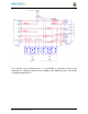
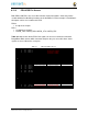
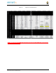
7.1.2 Connector P9
Table 12
lists the signals on connector
P9
. Other signals can be connected to this
connector based on setting the pin mux on the processor, but this is the default settings on
power up.
There are some signals that have not been listed here. Refer to the processor
documentation for more information on these pins and detailed descriptions of all of the
pins listed. In some cases there may not be enough signals to complete a group of signals
that may be required to implement a total interface.
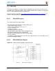
The
PROC
column is the pin number on the processor.
The
PIN
column is the pin number on the expansion header.
The
MODE
columns are the mode setting for each pin. Setting each mode to align with the
mode column will give that function on that pin.
NOTES:
In the table are the following notations:
PWR_BUT
is a 5V level as pulled up internally by the TPS65217C. It is activated by pulling
the signal to GND.
# Both of these signals connect to pin 41 of P11. Resistors are installed that allow for the
GPIO3_20 connection to be removed by removing R221. The intent is to allow the SW to
use either of these signals, one or the other, on pin 41. SW should set the unused pin in
input mode when using the other pin. This allowed us to get an extra signal out to the
expansion header.
@ Both of these signals connect to pin 42 of P11. Resistors are installed that allow for the
GPIO3_18 connection to be removed by removing R202. The intent is to allow the SW to
use either of these signals, on pin 42. SW should set the unused pin in input mode when
using the other pin. This allowed us to get an extra signal out to the expansion header.
NOTE: DO NOT APPLY VOLTAGE TO ANY I/O PIN WHEN POWER IS NOT
SUPPLIED TO THE BOARD. IT WILL DAMAGE THE PROCESSOR AND VOID THE
WARRANTY.
NO PINS ARE TO BE DRIVEN UNTIL AFTER THE SYS_RESET LINE GOES HIGH.