
Data Sheet


AM3359, AM3358, AM3357
AM3356, AM3354, AM3352
www.ti.com
SPRS717F –OCTOBER 2011–REVISED APRIL 2013
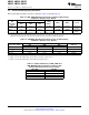
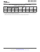
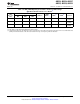
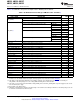
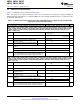
Table 3-12. Recommended Operating Conditions (continued)
PARAMETER
MIN NOM MAX UNIT
SUPPLY NAME DESCRIPTION
Voltage range for DDR SSTL and
DDR_VREF HSTL reference input (DDR2, 0.49*VDDS_DDR 0.50*VDDS_DDR 0.51*VDDS_DDR V
DDR3, DDR3L)
Voltage range for USB VBUS
USB0_VBUS 0.000 5.000 5.250 V
comparator input
Voltage range for USB VBUS
USB1_VBUS
(6)
0.000 5.000 5.250 V
comparator input
Voltage range for the USB ID
USB0_ID
(7)
V
input
Voltage range for the USB ID
USB1_ID
(6) (7)
V
input
Commercial Temperature 0 90
Operating Temperature
Industrial Temperature -40 90 °C
Range, T
j
Extended Temperature -40 105
(1) The supply voltage defined by OPP100 should be applied to this power domain before the device is released from reset.
(2) Not available on the ZCE package. VDD_MPU is merged with VDD_CORE on the ZCE package.
(3) This supply is sourced from an internal LDO when RTC_KALDO_ENn is low. If RTC_KALDO_ENn is high, this supply must be sourced
from an external power supply.
(4) VDDS should be supplied irrespective of 1.8-V or 3.3-V mode of operation of the dual-voltage IOs.
(5) For more details on power supply requirements, see Section 4.1.4.
(6) Not available on the ZCE package.
(7) This terminal is connected to analog circuits in the respective USB PHY. The circuit sources a known current while measuring the
voltage to determine if the terminal is connected to VSSA_USB with a resistance less than 10 Ω or greater than 100 kΩ. The terminal
should be connected to ground for USB host operation or open-circuit for USB peripheral operation, and should never be connected to
any external voltage source.
Copyright © 2011–2013, Texas Instruments Incorporated Device Operating Conditions 89
Submit Documentation Feedback
Product Folder Links: AM3359 AM3358 AM3357 AM3356 AM3354 AM3352