
Data Sheet


AM3359, AM3358, AM3357
AM3356, AM3354, AM3352
www.ti.com
SPRS717F –OCTOBER 2011–REVISED APRIL 2013
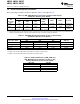
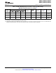
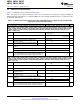
Table 3-9. VDD_CORE Operating Performance Points for ZCE Package
with Device Revision Code "A" or Newer
(1)
VDD_CORE VDD_MPU
(2)
OPP DDR3,
ARM (A8) DDR2
(3)
mDDR
(3)
L3 and L4
Rev "A" or DDR3L
(3)
MIN NOM MAX
newer
OPP100 1.056 V 1.100 V 1.144 V 600 MHz 400 MHz 266 MHz 200 MHz 200 MHz and
100 MHz
OPP100 1.056 V 1.100 V 1.144 V 300 MHz 400 MHz 266 MHz 200 MHz 200 MHz and
100 MHz
OPP50 0.912 V 0.950 V 0.988 V 300 MHz - 125 MHz 90 MHz 100 MHz and
50 MHz
(1) Frequencies in this table indicate maximum performance for a given OPP condition.
(2) VDD_MPU is merged with VDD_CORE on the ZCE package.
(3) This parameter represents the maximum memory clock frequency. Since data is transferred on both edges of the clock, double-data rate
(DDR), the maximum data rate is two times the maximum memory clock frequency defined in this table.
Copyright © 2011–2013, Texas Instruments Incorporated Device Operating Conditions 85
Submit Documentation Feedback
Product Folder Links: AM3359 AM3358 AM3357 AM3356 AM3354 AM3352