
Data Sheet


AM3359, AM3358, AM3357
AM3356, AM3354, AM3352
SPRS717F –OCTOBER 2011–REVISED APRIL 2013
www.ti.com
3 Device Operating Conditions
3.1 Absolute Maximum Ratings
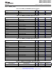
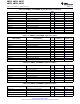
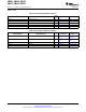
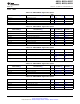
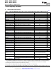
Table 3-1. Absolute Maximum Ratings Over Junction Temperature Range (Unless Otherwise Noted)
(1)(2)
PARAMETER MIN MAX UNIT
VDD_MPU
(3)
Supply voltage for the MPU core domain -0.5 1.5 V
VDD_CORE Supply voltage range for the core domain -0.5 1.5 V
CAP_VDD_RTC
(4)
Supply voltage range for the RTC core domain -0.5 1.5 V
VPP
(5)
Supply voltage range for the FUSE ROM domain -0.5 2.2 V
VDDS_RTC Supply voltage range for the RTC domain -0.5 2.1 V
VDDS_OSC Supply voltage range for the System oscillator -0.5 2.1 V
VDDS_SRAM_CORE_BG Supply voltage range for the Core SRAM LDOs -0.5 2.1 V
VDDS_SRAM_MPU_BB Supply voltage range for the MPU SRAM LDOs -0.5 2.1 V
VDDS_PLL_DDR Supply voltage range for the DPLL DDR -0.5 2.1 V
VDDS_PLL_CORE_LCD Supply voltage range for the DPLL Core and LCD -0.5 2.1 V
VDDS_PLL_MPU Supply voltage range for the DPLL MPU -0.5 2.1 V
VDDS_DDR Supply voltage range for the DDR IO domain -0.5 2.1 V
VDDS Supply voltage range for all dual-voltage IO domains -0.5 2.1 V
VDDA1P8V_USB0 Supply voltage range for USBPHY -0.5 2.1 V
VDDA1P8V_USB1
(6)
Supply voltage range for USBPHY -0.5 2.1 V
VDDA_ADC Supply voltage range for ADC -0.5 2.1 V
VDDSHV1 Supply voltage range for the dual-voltage IO domain -0.5 3.8 V
VDDSHV2
(6)
Supply voltage range for the dual-voltage IO domain -0.5 3.8 V
VDDSHV3
(6)
Supply voltage range for the dual-voltage IO domain -0.5 3.8 V
VDDSHV4 Supply voltage range for the dual-voltage IO domain -0.5 3.8 V
VDDSHV5 Supply voltage range for the dual-voltage IO domain -0.5 3.8 V
VDDSHV6 Supply voltage range for the dual-voltage IO domain -0.5 3.8 V
VDDA3P3V_USB0 Supply voltage range for USBPHY -0.5 4 V
VDDA3P3V_USB1
(6)
Supply voltage range for USBPHY -0.5 4 V
USB0_VBUS
(7)
Supply voltage range for USB VBUS comparator input -0.5 5.25 V
USB1_VBUS
(6)(7)
Supply voltage range for USB VBUS comparator input -0.5 5.25 V
DDR_VREF Supply voltage range for the DDR SSTL and HSTL -0.3 1.1 V
reference voltage
Steady State Max. Voltage
-0.5V to IO supply voltage + 0.3 V
at all IO pins
(8)
USB0_ID
(9)
Steady state maximum voltage range for the USB ID input -0.5 2.1 V
USB1_ID
(6)(9)
Steady state maximum voltage range for the USB ID input -0.5 2.1 V
Transient Overshoot and
25% of corresponding IO supply
Undershoot specification at
voltage for up to 30% of signal period
IO terminal
Storage temperature range,
-55 155 °C
T
stg
(10)
ESD-HBM (Human Body Model)
(11)
±2000
Electrostatic Discharge
V
(ESD) Performance
ESD-CDM (Charged-Device Model)
(12)
±500
Latch-up Performance
(13)
Class II (105°C) 45 mA
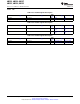
(1) Stresses beyond those listed under "absolute maximum ratings" may cause permanent damage to the device. These are stress ratings
only, and functional operation of the device at these or any other conditions beyond those indicated under "recommended operating
conditions" is not implied. Exposure to absolute-maximum-rated conditions for extended periods may affect device reliability.
(2) All voltage values are with respect to their associated VSS or VSSA_x.
(3) Not available on the ZCE package. VDD_MPU is merged with VDD_CORE on the ZCE package.
(4) This supply is sourced from an internal LDO when RTC_KALDO_ENn is low. If RTC_KALDO_ENn is high, this supply must be sourced
80 Device Operating Conditions Copyright © 2011–2013, Texas Instruments Incorporated
Submit Documentation Feedback
Product Folder Links: AM3359 AM3358 AM3357 AM3356 AM3354 AM3352