
Data Sheet


AM3359, AM3358, AM3357
AM3356, AM3354, AM3352
SPRS717F –OCTOBER 2011–REVISED APRIL 2013
www.ti.com
5.11.1.2 McSPI—Master Mode
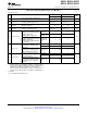
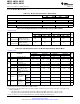
Table 5-83. McSPI Timing Conditions—Master Mode
LOW LOAD HIGH LOAD
TIMING CONDITION PARAMETER UNIT
MIN MAX MIN MAX
Input Conditions
t
r
Input signal rise time 8 8 ns
t
f
Input signal fall time 8 8 ns
Output Condition
C
load
Output load capacitance 5 25 pF
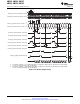
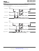
Table 5-84. Timing Requirements for McSPI Input Timings—Master Mode
(see Figure 5-90)
OPP100 OPP50
NO. LOW LOAD HIGH LOAD LOW LOAD HIGH LOAD UNIT
MIN MAX MIN MAX MIN MAX MIN MAX
Setup time, SPI_D[x]
4 t
su(SOMI-SPICLKH)
(SOMI) valid before 2.29 3.02 2.29 3.02 ns
SPI_CLK active edge
(1)
Hold time, SPI_D[x]
5 t
h(SPICLKH-SOMI)
(SOMI) valid after 4.7 4.7 4.7 4.7 ns
SPI_CLK active edge
(1)
(1) Pins SPIx_D0 and SPIx_D1 can function as SIMO or SOMI.
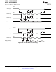
Table 5-85. Switching Characteristics for McSPI Output Timings—Master Mode
(see Figure 5-91)
OPP100 OPP50
UNI
NO. PARAMETER LOW LOAD HIGH LOAD LOW LOAD HIGH LOAD
T
MIN MAX MIN MAX MIN MAX MIN MAX
1 t
c(SPICLK)
Cycle time, SPI_CLK 20.8 20.8 41.6 41.6 ns
Typical Pulse duration,
2 t
w(SPICLKL)
0.5P
(1)
0.5P
(1)
0.5P
(1)
0.5P
(1)
0.5P
(1)
0.5P
(1)
0.5P
(1)
0.5P
(1)
ns
SPI_CLK low
Typical Pulse duration,
t
w(SPICLKH)
0.5P
(1)
0.5P
(1)
0.5P
(1)
0.5P
(1)
0.5P
(1)
0.5P
(1)
0.5P
(1)
0.5P
(1)
ns
SPI_CLK high
3
t
r(SPICLK)
Rising time, SPI_CLK 3.82 3.82 3.82 3.82 ns
t
f(SPICLK)
Falling time, SPI_CLK 3.44 3.44 3.44 3.44 ns
Delay time, SPI_CLK active
6 t
d(SPICLK-SIMO)
edge to SPI_D[x] (SIMO) -3.57 3.57 -4.62 4.62 -3.57 3.57 -4.62 4.62 ns
transition
(2)
Delay time, SPI_CS active
7 t
d(CS-SIMO)
edge to SPI_D[x] (SIMO) 3.57 4.62 3.57 4.62 ns
transition
(2)
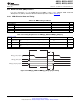
Mode 1
Delay time,
A - 4.2
(4)
A - 2.54
(4)
A - 4.2
(4)
A - 2.54
(4)
ns
and 3
(3)
SPI_CS active to
8 t
d(CS-SPICLK)
SPI_CLK first
Mode 0
B - 4.2
(5)
B - 2.54
(5)
B - 4.2
(5)
B - 2.54
(5)
ns
edge
and 2
(3)
Mode 1
Delay time,
B - 4.2
(5)
B - 2.54
(5)
B - 4.2
(5)
B - 2.54
(5)
ns
and 3
(3)
SPI_CLK last
9 t
d(SPICLK-CS)
edge to SPI_CS
Mode 0
A - 4.2
(4)
A - 2.54
(4)
A - 4.2
(4)
A - 2.54
(4)
ns
inactive
and 2
(3)
(1) P = SPI_CLK period.
(2) Pins SPIx_D0 and SPIx_D1 can function as SIMO or SOMI.
(3) The polarity of SPIx_CLK and the active edge (rising or falling) on which mcspix_simo is driven and mcspix_somi is latched is all
software configurable:
– SPIx_CLK(1) phase programmable with the bit PHA of MCSPI_CH(i)CONF register: PHA = 1 (Modes 1 and 3).
– SPIx_CLK(1) phase programmable with the bit PHA of MCSPI_CH(i)CONF register: PHA = 0 (Modes 0 and 2).
(4) Case P = 20.8 ns, A = (TCS+1)*TSPICLKREF (TCS is a bit field of MCSPI_CH(i)CONF register).
216 Peripheral Information and Timings Copyright © 2011–2013, Texas Instruments Incorporated
Submit Documentation Feedback
Product Folder Links: AM3359 AM3358 AM3357 AM3356 AM3354 AM3352