
User`s manual

Camera Functional Description
38 Basler aviator Camera Link
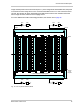
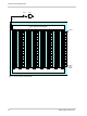
3.1.1 Four Tap Sensor Digitization Mode
With four tap sensor digitization, the sensor is divided into quadrants, and a separate electronic
circuit is used to read out the pixels in each quadrant (see Figure 15 on page 39). Each of the
electronic circuits used to read out a quadrant of the sensor is referred to as a tap. The advantage
of the four tap digitization scheme is that it makes readout very fast because the four circuits are
used simultaneously to read out the sensor.
After a image has been captured (i.e., exposure has ended), the pixels in the sensor become ready
to be read out. At readout, the accumulated charges are transported from the pixels to the sensor’s
vertical shift registers. The charges from the top line of pixels in the array are then moved to the
upper horizontal shift register and the charges from the bottom line of pixels are moved to the lower
horizontal shift register as shown in Figure 15. Once this has been accomplished, the following
operations are performed simultaneously:
Charges from the left half of the top line are moved out of the upper horizontal shift register.
The left half of the upper horizontal shift register shifts out charges from left to right, that is,
pixel 1, pixel 2, pixel 3, and so on.
Charges from the right half of the top line are moved out of the upper horizontal shift register.
The right half of the upper horizontal shift register shifts out charges from right to left, that is,
pixel n, pixel n-1, pixel n-2, and so on (where n is the last pixel in a line).
Charges from the left half of the bottom line are moved out of the lower horizontal shift register.
The left half of the lower horizontal shift register shifts out charges from left to right, that is,
pixel 1, pixel 2, pixel 3, and so on.
Charges from the right half of the bottom line are moved out of the lower horizontal shift
register. The right half of the lower horizontal shift register shifts out charges from right to left,
that is, pixel n, pixel n-1, pixel n-2, and so on (where n is the last pixel in a line).
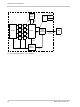
As the charges move out of the horizontal shift registers, they are converted to voltages proportional
to the size of each charge. Each voltage is then amplified by a Variable Gain Control (VGC) and
digitized by an Analog-to-Digital converter (ADC). For optimal digitization, gain and black level can
be adjusted by setting camera parameters.
After each voltage has been amplified and digitized, it passes through an FPGA and into an image
buffer. All shifting of charges from the vertical to the horizontal registers and out of the horizontal
registers is clocked according to the camera’s internal data rate. Shifting continues until all image
data has been read out of the sensor.
As the pixel data passes through the FPGA and into the buffer, it is reordered so that the pixel data
for each line is in ascending order from pixel 1 through pixel n.
There are two "Camera Link tap geometries" that can be used to determine how the pixel data in
the image buffer will be transmitted over the Camera Link interface to the frame grabber in your PC.
The first tap geometry is called 1X2-1Y. When 1X2-1Y is selected, the pixel data in the image buffer
will be transmitted line-by-line in ascending order from line one through the last line in the image. If
the camera is set for 1X2-1Y, the entire image must be read out of the imaging sensor and stored
in the image buffer before the camera can begin to transmit pixel data via the Camera Link interface.
The second tap geometry is called 1X-2YE. When 1X-2YE is selected, the pixel data in the image
buffer will be transmitted in a different fashion. First, the pixels in the first line in the image and pixels
in the last line (line n) in the image will be transmitted. Next, the pixels in the second line of the