
User's Manual

Page 3 of 5
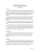
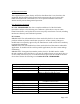
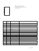
RM912HP Schematic
Connection Diagram and
Instructions.
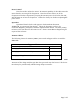
Pin # Pin
Name
Pin Function Connection Instructions
1 G1 RF Ground Via directly to ground.
2 RF RF Signal Route a 50 ohm trace to the antenna.
3 G3 RF Ground Via directly to ground.
4 SW1 Switch 1 ctrl – active low Tx Logic low for Tx, high for Rx
5 SW2 Switch 2 ctrl – active low Rx Logic high for Tx, low for Rx
6 V Vdd, general purpose
supply
Supply 2.7 V, +/- 10%
7 G2 Ground Signal ground
8 TP2 Power Amp Enable Power amp enable.
9 Reset Transceiver ~RST See Transceiver datasheet.
10 Select Transceiver ~SEL (for SPI) See Transceiver datasheet.
11 MISO Transceiver Data Out SPI data out of Transceiver
12 MOSI Transceiver Data In SPI data in to Transceiver
13 SCLK Transceiver SPI Clock SPI Clock, see Transceiver datasheet for usage guidelines.
14 DIG2 Transceiver DIG2 See Transceiver datasheet.
15 G4 Ground Signal ground
16 V2 Power Amp VCC Supply 1.5 – 2.7 V during transmit
17 LNA Bias LNA Enable Low = ON, HI-Z = OFF
18 LNA Gain LNA Gain Control High for high linearity, low for high gain.
19 SLP_TR Atmel SLP_TR See Transceiver datasheet; pulse high to initiate Tx
20 IRQ Atmel IRQ Various interrupt sources
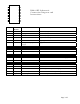
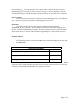
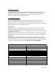
1
2
3
4
5
6
7
8
9
10
17
16
15
14
13
12
11
20
19
18