
Product Info


B&R wireless board "RFM-2-NF"
Standard Documentation for Radio Equipment Certification
Block diagram
Copyright © B&R - Subject to modification
Description Module RFM-2-NF_1_Version 1.4.docx
Tuesday, April 9, 2019 2:25:00
PM
6/17
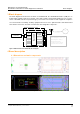
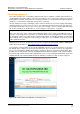
3 Block diagram
The block diagram shows the basic elements of the RFM-2-NF, the standardized interface (USB), the on
board voltage regulator and the used parts of the SRD controller. Permanently disabled or not used ele-
ments of the SRD controller are pictured in grey color and are not relevant for radio equipment compliance
assessment. Same for auxiliary, ancillary equipment and accessories. Optical interface, RC-Network and
Host Interface Connector should be considered as interchangeable components.
Figure 3: B&R wireless board “RFM-2-NF” block diagram
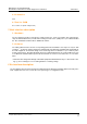
4 Board description
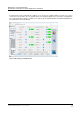
4.1 Dimensions and main components
Figure 4: B&R wireless board “RFM-2-NF” front view (component side), L x W = 95 x 24 mm
Figure 5: B&R wireless board “RFM-2-NF” diaphanous view (solder side and component side)
Shielding, housing of module
SRD controller (Elatec TWN4)
Host Interface
Connector
Host
Interface
USB
Voltage
regulator
RFID
HF-Interface
13.56 MHz
RFID
LF-Interface
125 kHz/134kHz
CAN
I²C
ECI
SPI
Serial
GPIO
SAM2
SAM1
Sound
Micro Control Unit
(radio control unit)
RC-Network
Optical interface
RFID HF-Interface:
Transmitting lines: Pin1, 3, 5
Receiving lines: Pin2, 6
Frequency flow:
oscillators only inside the
shielded SRD controller
TAG
air interface
communications