
User Manual

Airborne DP550 Family Databook B&B Electronics, Inc.
9
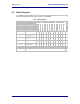
5.0 Pin out and Connectors
Pin definition is dependent upon the device type selected. The specific pin function is
defined in Table 2 for each device type. Where multiple options are available for a single
device type, these options are software selectable by the device firmware.
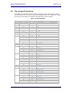
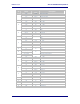
Table 2 – Module Pin Definition
Pin Name
Device
Type
Description
1 GND All Digital Ground
2 TDI All JTAG: Test data in
3 VDD All 3.3VDC
4 VDD All 3.3VDC
5 RTCK All JTAG: Return Test Clock
6 DTXD All D
OUT
Debug
7 /RESET All Module RESET
8 DRXD All D
IN
Debug
9
RXD2 UART D
IN
UART2
RXD2 Serial D
IN
UART2
RXD2 SPI D
IN
UART2
RXD2 Ethernet D
IN
UART2
G6 All GPIO
10 TDO All JTAG: Test data out
11 /FRESET All Factory RESET
12
CTS1 UART Clear-to-Send UART1
CTS Serial Clear-to-Send
/SPI_SEL SPI SPI Select
CTS1 Ethernet Clear-to-Send UART1
F5 All GPIO
13
NC UART No Connect
NC Serial No Connect
NC SPI No Connect
RX+ Ethernet Ethernet RX+
14
NC UART No Connect
NC Serial No Connect
NC SPI No Connect
RX- Ethernet Ethernet RX-
15 GND All Digital Ground
16 GND All Digital Ground
17
RTS2 UART Ready-to-Send UART2
/TXEN Serial Line Driver Tx enable
RTS2 SPI Ready-to-Send UART2
RTS2 Ethernet Ready-to-Send UART2
G2 All GPIO
18
RTS1 UART Ready-to-Send UART1
RTS Serial Ready-to-Send
SPI_CLK SPI SPI Clock Input
RTS1 Ethernet Ready-to-Send UART1
F4 All GPIO
19 CTS2 UART Clear-to-Send UART2