
User's Manual

Quatech, Inc. Company Confidential
Revision 1.0 100-8026-100G Airborne 802.11b/g Value Radio Databook 29
11.4 Circuit Board Layout Guidelines
When considering capacitance, calculations must consider all device loads and
capacitances due to printed circuit board traces. Capacitance due to the traces
depend on a number of factors, including the trace width, dielectric material from
which the circuit board is made, and proximity to ground and power planes.
The mating connector required on the host board is a DF12(4.0)-50DP-0.5, the
manufacturer is Hirose.
11.5 Mounting Guidelines
Special care must be observed when placing the Module. In particular:
The antenna must not be mounted beneath any other printed circuit boards,
components, or metallic housing.
The proximity of the antenna to large metallic objects can affect the range
and performance of the Module.
Packaging and enclosure designers must carefully review the placement of
the Module in the enclosure to minimize interference or blocking sources
.
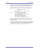
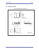
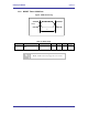
For mechanical clearance, performance, and emissions reasons, there should be
no components placed on the main printed circuit board facing the Module. This
area should be clear of any components. The recommended mounting footprint
for the radios can be seen in Figure 5.
Figure 5 - WLRG-RA-DP101 Mounting Footprint
Radio PCB Outline
0.630 [16.00]
0.413 [10.50]
0.004 [0.10]
Dimensions: inches [mm]
PC16 (CF) Header
1
250
49
.827 [21.00]
.118 [3.00]
1.063 [27.00]
Ø.086 [Ø2.18]
1.260 [32.00]
.118 [3.00]
1.496 [38.00]
.295 [7.48]