
Data Sheet


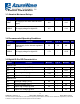


Table Of Contents

12
FORM NO.: FR2-015_ A Responsible Department:WBU Expiry Date: Forever
The information contained herein is the exclusive property of AzureWave and shall not be distributed, reproduced, or disclosed
in whole or in part without prior written permission of AzureWave.
2.2 Pin Table
Pin No
Definition
Basic Description
Voltage
Type
1
GND
Ground.
GND
2
WL_BT_ANT
WLAN/BT RF TX/RX path.
RF
3
GND
Ground.
GND
4
NC
Floating Pin, No connect to anything.
Floating
5
NC
Floating Pin, No connect to anything.
Floating
6
BT_WAKE
BT Device Wake
I
7
BT_HOSTWAKE
BT Host Wake
O
8
NC
Floating Pin, No connect to anything.
Floating
9
VBAT
3.3V power pin
3.3V
VCC
10
GND
Ground.
GND
11
GND
Ground.
GND
12
WL_REG_ON
Used by PMU to power up or power down the
internal regulators used by the WLAN section.
Also, when deasserted, this pin holds the WLAN
section in reset. This pin has an internal 200k ohm
pull down resistor that is enabled by default. It can
be disabled through programming.
I
13
WL_SDIO_HOST
WAKE
WL Host Wake
O
14
SDIO_DATA2
SDIO Data Line 2
I/O
15
SDIO_DATA3
SDIO Data Line 3
I/O
16
SDIO_CMD
SDIO Command Input
I/O
17
SDIO_CLK
SDIO Clock Input
I
18
SDIO_DATA0
SDIO Data Line 0
I/O
19
SDIO_DATA1
SDIO Data Line 1
I/O
20
GND
Ground.
GND
21
VIN_LDO_OUT
Internal Buck voltage generation pin
1.35V(typ)
VCC
22
VDDIO
1.8V-3.3V VDDIO supply for WLAN and BT
VIO
VCC
23
VIN_LDO
Internal Buck voltage generation pin
1.35V(typ)
VCC
24
SUSCLK_IN
External 32K or RTC clock
I
25
BT_PCM_OUT
PCM data Out
O
26
BT_PCM_CLK
PCM Clock
I/O
27
BT_PCM_IN
PCM data Input
I
28
BT_PCM_SYNC
PCM Synchronization control
I/O
29
GPIO_7
SDIO mode selection pin
1.8V:pull up, connect to 1.8V
3.3V:pull down, connect to GND with using a 10K
resistor or less
I
30
GPIO_4
GPIO configuration pin
I/O
31
GND
Ground.
GND
32
NC
Floating Pin, No connect to anything.
Floating