
Data Sheet

17
● DMA support
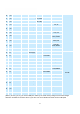
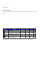
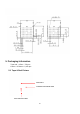
3.8.1 SPI Timing
The timing of the SPI interface when the SPI controller is in Slave mode is presented in below
figure.
Symbol Parameter Minimum Typical
Maximu
m
Unit
t
CKPER
spi_clk clock period 0.25 * ns
t
CSST
CS active time before rising edge 10.6 +T
INT
5.2 + T
INT
3.1 + T
INT
ns
t
CSHOLD
CS active time after falling edge 0 0 0 ns
t
MOST
Input data latching setup time 2.7 1.5 0.9 ns
t
MOHOLD
Input data hold time 0 0 0 ns
t
SODEL
Output data hold time 17.2 8.6 5.5 ns
Note TINT represents the internal SPI clock period and is equal to 1.5 * spi_clk period.