
Handbook
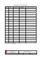


Table Of Contents
- AMENDMENT LIST RECORD SHEET
- INTRODUCTION
- 1.SAFETY CONSIDERATIONS
- 2.OVERVIEW/SYSTEM DESCRIPTION
- 3.SPECIFICATIONS
- 3.1Parts Lists
- 3.2Technical Specifications
- 3.2.1UHF ONE to Tunnels 1 & 2 Technical Specification
- 3.2.2UHF1A Technical Specification
- 3.2.3UHF ONE to Location TWO Technical Specification
- 3.2.4UHF TWO to Tunnels 1 & 2 Technical Specification
- 3.2.5UHF TWO to Location TWO Technical Specification
- 3.2.6800MHz Bi-directional Amplifier to Location TWO Technical Specification
- 3.3Mechanical Specification (UHF1/1A & UHF2 Wall Cases)
- 4.SYSTEM DRAWINGS
- 5.SUB-UNIT MODULES
- 5.1UHF 1 Air Interface (60-055901)
- 5.1.1Bandpass Duplexers (02-013401)
- 5.1.22 & 4 Way UHF Splitters (05-002603 & 05-003401)
- 5.1.3¼Watt 0- -30dB Switched Attenuator \(10-00
- 5.1.4Low Noise Amplifiers (11-006102, 11-007302 & 11-007402)
- 5.1.4.1General Description
- 5.1.4.2Technical Specification (11-006102)
- 5.1.4.3Drg. No. 11-006102, Low Noise Amplifier General Assembly
- 5.1.4.4Drg. No. 11-006170, LNA RF Circuit Diagram
- 5.1.4.5Drg. No. 11-006171, LNA DC Wiring Diagram
- 5.1.4.6Drg. No. 11-003971, LNA DC Schematic Diagram
- 5.1.4.7Technical Specification (11-007302)
- 5.1.4.8Drg. No. 11-007302, LNA Assembly With Alarm Relay
- 5.1.4.9Drg. No. 11-007370, LNA RF Circuit Diagram
- 5.1.4.10Drg. No. 11-007371, LNA DC Wiring Diagram
- 5.1.4.11Technical Specification (11-007402)
- 5.1.4.12Drg. No. 11-007402, LNA General Assembly
- 5.1.4.13Drg. No. 11-007470, LNA RF Circuit Diagram
- 5.1.4.14Drg. No. 11-007471 LNA DC Wiring Diagram
- 5.1.55Watt Power Amplifier (12-001801)
- 5.1.5.1Description
- 5.1.5.2Technical Specification
- 5.1.5.3Drg. No. 12-001801, 5Watt PA General Assembly Drawing
- 5.1.5.4Drg. No. 12-001870, 5Watt PA Circuit Diagram
- 5.1.5.5Drg. No. 12-001870C1, 5W PA Component List(1)
- 5.1.5.6Drg. No. 12-001870C2, 5W PA Component List(2)
- 5.1.5.7Drg. No. 80-008450, Power Amplifier/Alarm Board DC Wiring Details
- 5.1.63 Stage Amplifier Alarm Boards (12-002201)
- 5.1.7DC/DC Converter, 24V in, 12V 8A out (13-003011)
- 5.1.8Channel Selective & Channel Control Modules (17-003012 & 17-002101)
- 5.1.8.1Channel Selective Module Description
- 5.1.8.2Drg. No. 17-003080, Generic Channel Module Block Diagram
- 5.1.8.3Channel Selectivity Control Module Description
- 5.1.8.4Channel Controller DIP Switch Configuration Frequencies
- 5.1.8.5UHF1 Downlink Channel Module Configuration Table
- 5.1.8.6UHF1 Uplink Channel Module Configuration Table
- 5.1.8.7UHF1A Downlink Channel Module Configuration Table
- 5.1.8.8UHF1A Uplink Channel Module Configuration Table
- 5.1.8.9UHF2 Downlink Channel Module Configuration Table
- 5.1.8.10UHF2 Uplink Channel Module Configuration Table
- 5.1.9Single & Dual 24Volt Relay Boards (20-001602 & 80-008902)
- 5.1.10SMA coaxial termination (93-930003)
- 5.1.1124V 400W Flat-Pack Power Supply (96-300011)
- 5.2UHF 2 Air Interface (60-055902)
- 5.2.1Bandpass Filter (02-013401) See section 5.1.1
- 5.2.24 Port Tx Hybrid Combiner (05-003019)
- 5.2.3Four Way Low Power Splitter (05-003401) See section 5.1.2
- 5.2.4¼Watt 0- -30dB Switched Attenuator \(10-00
- 5.2.5Low Noise Amplifiers (11-007302 & 11-007402) See section 5.1.4
- 5.2.63 Stage Amplifier Alarm Boards (12-002201) See section 5.1.6
- 5.2.720Watt Power Amplifier (12-004201)
- 5.2.8DC/DC Converter, 24V in, 12V 8A out (13-003011) See section 5.1.7
- 5.2.9Chan. Selec. & Chan. Contr. Mdls (17-003012 & 17-002101) See section 5.1.8
- 5.2.1021MHz IF Filter Board (17-002502)
- 5.2.11Single & Dual 24Volt Relay Boards (20-001602 & 80-008902) See section 5.1.9
- 5.2.12SMA Coaxial Termination (93-930003) See section 5.1.10
- 5.2.1324V 400W Flat-Pack Power Supply (96-300011) See section 5.1.11
- 5.2.14JWS75-15/A PSU (96-300045)
- 5.2.15Single Mode Optical Coupler (98-100001)
- 5.2.16.Fibre Optic Receiver & Transmitter (98-200003 & 98-300003)
- 5.3UHF1A 60-055903 470MHz 3 Channel BDA
- 5.1UHF 1 Air Interface (60-055901)
- 6.INSTALLATION
- 7.MAINTENANCE
- APPENDIX AINITIAL EQUIPMENT SET-UP CALCULATIONS

PBL UHF1/1A 1 & 2 Air Interface
Maintenance Handbook
H/book Number:-60-055900HBKM
Issue No:-2
Date:-20/10/2003
Page:-
4 of 85
5.2.7.1 Description .......................................................................................................................................68
5.2.7.2 Technical Specification ....................................................................................................................68
5.2.7.3 Drg. Nō. 12-004201, PA General Assembly....................................................................................69
5.2.7.4 Drg. Nō. 12-004270, PA Circuit Diagram .......................................................................................70
5.2.7.5 Drg. Nō. 12-004270C1, PA Parts List(1).........................................................................................71
5.2.7.6 Drg. Nō. 12-004270C2, PA Parts List(2).........................................................................................72
5.2.7.7 Drg. Nō. 12-003670, PA to Alarm Wiring Details ..........................................................................73
5.2.8 DC/DC Converter, 24V in, 12V 8A out (13-003011) See section 5.1.7..................................................74
5.2.9 Chan. Selec. & Chan. Contr. Mdls (17-003012 & 17-002101) See section 5.1.8 ...................................74
5.2.10 21MHz IF Filter Board (17-002502)....................................................................................................74
5.2.10.1 Description ...................................................................................................................................74
5.2.11 Single & Dual 24Volt Relay Boards (20-001602 & 80-008902) See section 5.1.9.............................74
5.2.12 SMA Coaxial Termination (93-930003) See section 5.1.10 ................................................................74
5.2.13 24V 400W Flat-Pack Power Supply (96-300011) See section 5.1.11 .................................................74
5.2.14 JWS75-15/A PSU (96-300045)............................................................................................................74
5.2.14.1 Description ...................................................................................................................................74
5.2.14.2 Technical Specification ................................................................................................................74
5.2.15 Single Mode Optical Coupler (98-100001)..........................................................................................75
5.2.15.1 Description ...................................................................................................................................75
5.2.16. Fibre Optic Receiver & Transmitter (98-200003 & 98-300003) .........................................................75
5.2.16.1 Description ...................................................................................................................................75
5.2.16.2 Technical Specification ................................................................................................................76
5.3 UHF1A 60-055903 470MHZ 3 CHANNEL BDA.........................................................................................77
6. INSTALLATION............................................................................................................................ 78
6.1 INITIAL INSTALLATION RECORD ................................................................................................................78
6.2 GENERAL .....................................................................................................................................................78
6.3 ELECTRICAL CONNECTIONS .......................................................................................................................78
6.4 OPTICAL CONNECTIONS..............................................................................................................................78
6.5 RF CONNECTIONS .......................................................................................................................................79
6.6 COMMISSIONING..........................................................................................................................................79
7. MAINTENANCE............................................................................................................................ 80
7.1 GENERAL PROCEDURES ..............................................................................................................................80
7.1.1 Fault Finding ............................................................................................................................................80
7.1.2 Downlink..................................................................................................................................................81
7.1.3 Uplink.......................................................................................................................................................81
7.1.4 Fault repair ...............................................................................................................................................81
7.1.5 Checking service ......................................................................................................................................82
7.1.6 Service Support ........................................................................................................................................82
7.2 TOOLS & TEST EQUIPMENT........................................................................................................................82
7.3 CARE OF MODULES .....................................................................................................................................83
7.3.1 General Comments...................................................................................................................................83
7.3.2 Module Removal (LNA’s, general procedure): .......................................................................................83
7.3.3 Module Replacement (general): ...............................................................................................................83
7.3.4 Power Amplifiers .....................................................................................................................................83
7.3.5 Low Power Amplifier Replacement.........................................................................................................84
7.3.6 Module Transportation:............................................................................................................................84
APPENDIX A INITIAL EQUIPMENT SET-UP CALCULATIONS............................................... 85