
User Instructions

RDA5856TE
Copyright@2016 RDA Microelectronics. CONFIDENTIAL 6 / 17
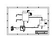
3. Function Block Diagram
I2C
Master
Debug
Host
UART SD/MMC PWM
USB 2.0
OTG
GPIO AIF
VOC
MCU
VOC
MEM
MCU
RAM
MCU
RAM
DMA
BT
Baseband
FM
Analog Audio
CODEC
BT
Radio
BT_ANT
FM_ANT
Line In
MIC In
DAC Out
PMU
Flash
Controller
DP/DN
PMW
out x4
SD UARTUARTHST_CLK
I2C
GPIO
Serial
Flash
Figure 2 RDA5856TE Block Diagram
4. Clock and reset
RDA5856TE has a reference clock input from either a crystal or an external clock source. There are
two internal PLL which use XTAL clock as reference. They are used for system and audio
applications.
SYSPLL
AUDPLL DIV
clk_codec
clk_sys
XTAL
Figure 3 Clock Structure
RDA5856TE has several reset sources, as following:
POR
Entire SoC is reset after power supply ramping from 0v to VBAT.
External Pin Reset
Entire SoC is reset except PMU.
Warm Reset
Global soft reset
DBB can be reset by set soft reset register in system control register map.
Watch Dog Reset
DBB will be reset when watch dog timer expired.
5. MCU
RDA RISC is a 16/32-bits processor which using a Reduced Instruction Set Architecture, an efficient
6-stage instruction pipeline, it provides high performance to the system.
RDA RISC Core.
32x32-bit Multiplier.