
Manual

EEV-EX03
26 EEV-EX03 Quick Installation Guide
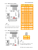
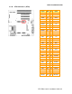
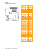
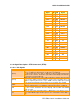
Signal PIN
PIN
Signal
TRDY# A61
A62
USB3-
IRDY#
A63
A64
STOP#
FRAME# A65
A66
USB2+
GND
A67
A68
GND
AD16 A69
A70
CBE#2
AD17
A71
A72
USB3+
AD19 A73
A74
AD18
AD20
A75
A76
USB0-
AD22 A77
A78
AD21
AD23
A79
A80
USB1-
AD24 A81
A82
CBE#3
+5V
A83
A84
+5V
AD25 A85
A86
AD26
AD28
A87
A88
USB0+
AD27 A89
A90
AD29
AD30
A91
A92
USB1+
PCIRST# A93
A94
AD31
INTR#C
A95
A96
INTR#D
INTR#A A97
A98
INTR#B
GND
A99
A100
GND
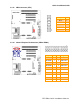
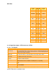
2.3.27 Signal Description – ETX Connector 1 (ETX1)
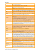
2.3.27.1 PCI Signals
Signal Signal Description
PCICLK [1:4]
PCI clock outputs for up to 4 external PCI slots or devices.
The baseboard designer should route these clocks for 1300pS total delay from the
ETX connector pin to the clock pin of the PCI device. See the ETX Design Guide
for typical route length calculations.
REQ [0:3]#
Bus Request signals for up to 4 external bus mastering PCI devices. When
asserted, a PCI device is requesting PCI bus ownership from the arbiter.
GNT [0:3]#
Grant signals to PCI Masters. When asserted by the arbiter, the PCI master has
been granted ownership of the PCI bus.
AD [0:31]
PCI Address and Data Bus Lines. These lines carry the address and data
information for PCI transactions.
CBE [0:3]#
PCI Bus Command and Byte Enables. Bus command and byte enables are
multiplexed in these lines for address and data phases, respectively.
PAR
Parity bit for the PCI bus. Generated as even parity across AD [31:0] and CBE
[3:0]#.
SERR#
System Error. Asserted for hardware error conditions such as parity errors
detected in DRAM.
PERR# Parity Error. For PCI operation per exception granted by PCI 2.1 Specification.