
User guide


Spartan-6 FPGA Configuration User Guide www.xilinx.com 55
UG380 (v2.7) October 29, 2014
Board Layout for Configuration Clock (CCLK)
• Terminate the end of the CCLK transmission line with a parallel termination of 100Ω
to V
CCO
and 100Ω to GND (the Thevenin equivalent of V
CCO
/2, and assuming a trace
characteristic impedance of 50Ω).
• After configuration in master mode, the CCLK pin is not driven unless it is used in the
user design. If unused in the design, it is recommended to drive this pin to a logic
level to prevent the pin from floating after configuration has completed.
Familiarity with the advantages and disadvantages of available termination techniques
helps the designer choose the best option for the target application. Refer to UG393
,
Spartan-6 FPGA PCB Design and Pin Planning Guide, for detailed guidelines to determine
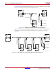
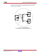
the appropriate topology for the intended application and detailed trade-offs. Figure 2-22
through Figure 2-24 show a few possible topologies for CCLK distribution. Because the
Master CCLK goes to high impedance at the end of the configuration sequence, the
examples using parallel termination can be less desirable than other termination options
because more power is dissipated. This trade-off must be weighed against other factors to
determine the optimal termination topography for an interface.
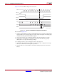
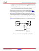
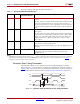
Figure 2-22 through Figure 2-25 show the recommended topologies for CCLK distribution.
Figure 2-22 shows the basic point-to-point topology for one CCLK driver (FPGA master)
and one CCLK receiver (PROM or FPGA slave).
X-Ref Target - Figure 2-22
Figure 2-22: Point-to-Point: One CCLK Output, One CCLK Input
CCLK Output = Master FPGA
CCLK Input = PROM or Slave FPGA
CCLK
Output
UG380_c2_21_062510
Z
0
(50Ω)
CCLK
Input
Z
0
(50Ω)
2 x Z
0
(100Ω)
2 x Z
0
(100Ω)
V
CCO_2