
User guide

54 www.xilinx.com Spartan-6 FPGA Configuration User Guide
UG380 (v2.7) October 29, 2014
Chapter 2: Configuration Interface Basics
• Hold the FPGA PROGRAM_B pin Low from power-up to delay the start of the FPGA
configuration procedure and release the PROGRAM_B pin to High after the parallel
NOR flash is fully powered and is able to perform asynchronous reads.
• Hold the FPGA INIT_B pin Low from power-up to delay the start of the FPGA
configuration procedure and release the INIT_B pin to High after the parallel NOR
flash becomes ready for asynchronous reads.
External Configuration Clock for Master Modes
By default, Spartan-6 FPGAs perform master mode configuration using an internally
generated clock source. However, Spartan-6 FPGAs support the ability to dynamically
switch to an external clock source during master mode configuration. The external clock
source is effective for an application where faster and stable configuration times are
needed.
USERCCLK is a dual-purpose pin that can be used by the application as GCLK0 after the
configuration. To enable the external clock source during master mode configuration, the
ExtMasterCclk_en option in BitGen must be enabled. The USERCCLK frequency can be
divided down using the ExtMasterCclk_divide BitGen option. The allowable values
are 1 (default) and all even numbers between 2 and 1022. The I/O standard for the
USERCCLK is LVCMOS 8 mA slow slew rate. The configuration begins with the CCLK
generated by the FPGA internal oscillator. When the configuration clock register setting is
reached in the bitstream, the FPGA switches from the internal oscillator to the clock found
on USERCCLK (or divided down, as set by the BitGen option ExtMasterCclk_divide).
The clock multiplexer is designed to generate a glitchless output clock during the
transition. Care must be exercised when also using this clock output as an input to the
design. When the end of startup (EOS) completes, the I/O standard for this pin as specified
by the design is enabled. At this time, the input of this pin might glitch as the I/O changes
from the default I/O standard to the user-specified I/O standard.
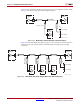
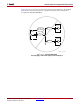
Board Layout for Configuration Clock (CCLK)
The Spartan-6 FPGA configuration I/Os use the LVCMOS slow slew rate 8 mA I/O
standard. This requires more attention to PCB trace routing and termination for proper
signal integrity.
These basic guidelines must be followed:
• Route the CCLK net as a 50Ω controlled impedance transmission line.
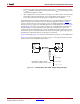
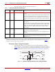
• Always route the CCLK net without any branching; do not use a star topology
(Figure 2-25).
• Stubs, if necessary, must be shorter than 8 mm (0.3 inches).
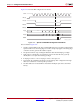
Table 2-8: Spartan-6 FPGA External Configuration Clock Interface Pin
Pin Name Type
Dedicated or
Dual-Purpose
Description
USERCCLK Input Dual-purpose External
configuration clock
source for all master
configuration modes