
User guide


Spartan-6 FPGA Configuration User Guide www.xilinx.com 53
UG380 (v2.7) October 29, 2014
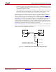
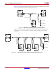
Master BPI Configuration Interface
Determining the Maximum Configuration Clock Frequency
In Master BPI mode, the FPGA delivers the configuration clock. The master configuration
clock frequency of the FPGA is set through the BitGen -g ConfigRate option. The
BitGen -g ConfigRate option sets the nominal configuration clock frequency. The
default BitGen ConfigRate setting of 2 is recommended. This default value sets the
nominal master CCLK frequency to 2 MHz, which satisfies timing requirements for the
leading BPI flash families. If the timing requirements discussed in this section are satisfied,
the BitGen ConfigRate setting can be increased for a faster configuration time. When
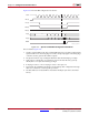
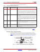
determining a valid ConfigRate setting, these timing parameters must be considered:
• FPGA nominal master CCLK frequency (BitGen ConfigRate)
• FPGA Master CCLK frequency tolerance (FMCCKTOL)
• A[25:0] outputs valid after CCLK falling edge (TBPICCO)
• BPI flash address to output valid (access) time (TACC)
• FPGA data setup time to CCLK rising edge (TBPIDCC)
The master configuration clock of the FPGA has a tolerance of FMCCKTOL. Due to the
master configuration clock tolerance (FMCCKTOL), the BitGen -g ConfigRate option
must be checked so that half the period for the worst-case (fastest) master CCLK frequency
is greater than the sum of the FPGA address valid time, BPI flash access time, and FPGA
set up time, as shown in Equation 2-1.
Equation 2-1
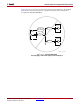
Power-On Sequence Precautions
At power-on, the FPGA automatically starts its configuration procedure. When the FPGA
is in a Master-BPI configuration mode, the FPGA asserts FCS_B Low and drives a sequence
of addresses to read the bitstream from a parallel NOR flash. The parallel NOR flash must
be ready for asynchronous reads before the FPGA drives FCS_B Low and outputs the first
address to ensure the parallel NOR flash can output the stored bitstream.
Because different power rails can supply the FPGA and parallel NOR flash or because the
FPGA and parallel NOR flash can respond at different times along the ramp of a shared
power supply, special attention to the FPGA and parallel NOR flash power-on sequence or
power-on ramps is essential. The power-on sequence or power supply ramps can cause the
FPGA to awake before the parallel NOR flash or vice versa. For many systems with near-
simultaneous power supply ramps, the FPGA power-on reset time (T
POR
) can sufficiently
delay the start of the FPGA configuration procedure such that the parallel NOR flash
becomes ready before the start of the FPGA configuration procedure. In general, the
system design must consider the effect of the power sequence, the power ramps, FPGA
power-on reset time, and parallel NOR flash power-on reset time on the timing relation
between the start of FPGA configuration and the readiness of the parallel NOR flash for
asynchronous reads. Check DS162
, Spartan-6 FPGA Data Sheet: DC and Switching
Characteristics, for Spartan-6 FPGA power supply requirements and timing.
One of the following system design approaches can ensure that the parallel NOR flash is
ready for asynchronous reads before the FPGA starts its configuration procedure:
• Control the sequence of the power supplies such that the parallel NOR flash is certain
to be powered and ready for asynchronous reads before the FPGA begins its
configuration procedure.
1
2 ConfigRate× FMCCKTOLMAX×
------------------------------------------------------------------------------------------------
TBPICCO TACC TBPIDCC++≥