
User guide

Spartan-6 FPGA Configuration User Guide www.xilinx.com 47
UG380 (v2.7) October 29, 2014
Master BPI Configuration Interface
configuration procedure such that the SPI flash becomes ready before the start of the FPGA
configuration procedure. In general, the system design must consider the effect of the
power sequence, the power ramps, FPGA power-on reset timing, and SPI flash power-up
timing on the timing relationship between the start of FPGA configuration and the
readiness of the SPI flash. Check DS162
, Spartan-6 FPGA Data Sheet: DC and Switching
Characteristics, for Spartan-6 FPGA power supply requirements and timing. Check the SPI
flash data sheet for the SPI flash power-up timing requirements.
One of the following system design approaches can ensure that the SPI flash is ready to
receive commands before the FPGA starts its configuration procedure:
• Control the sequence of the power supplies such that the SPI flash is certain to be
powered and ready for asynchronous reads before the FPGA begins its configuration
procedure.
• Hold the FPGA PROGRAM_B pin Low from power-up to delay the start of the FPGA
configuration procedure and release the PROGRAM_B pin to High after the SPI flash
is fully powered and is able to receive commands.
• Hold the FPGA INIT_B pin Low from power-up to delay the start of the FPGA
configuration procedure and release the INIT_B pin to High after the SPI flash
becomes ready to receive commands.
For more information on how to configure FPGAs with SPI flash and how to use iMPACT
software perform in-system SPI programming, see XAPP951
, Configuring Xilinx FPGAs
with SPI Serial Flash.
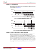
SPI Serial Daisy-Chain
In a serial daisy-chain application, the leading device can be in SPI mode and all
downstream devices in Slave Serial mode. In this case, all configuration bitstreams can be
stored inside one SPI device. The bitstream format for Master and Slave Serial daisy-chains
is exactly the same. See Serial Daisy-Chains, page 145 for details.
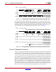
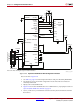
Master BPI Configuration Interface
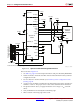
In the Master Byte-wide Peripheral Interface (BPI) shown in Figure 2-19, the Spartan-6
FPGA can configure itself from an industry-standard parallel NOR flash, as illustrated in
Figure 2-20. Spartan-6 FPGAs support up to 1 Gb parallel NOR flash, which can be
accessed with up to 26 address signals. Refer to the specific Spartan-6 device and package
to determine the number of address signals that limit the maximum flash density for
configuration.
Some BPI considerations are:
• The memory controller block in bank 1 (MCB-M1) cannot be used when the Master
BPI configuration interface is targeted. The design can either use the dual-purpose
pins for the MCB or for the BPI configuration interface but not both.
• 6SLX25/T devices do not support the BPI interface.
• 6SLX4 devices and Spartan-6 FPGAs in TQG144 and CPG196 packages do not
support the BPI interface.
• In the CSG225 package, address configuration pins A22 and A23 are not available.
The iMPACT programming software provides the ability to program top or bottom boot
parallel NOR flash using an indirect programming method. A small piece of IP is required
to be added to the FPGA design that provides a connection from the iMPACT software