
User guide

46 www.xilinx.com Spartan-6 FPGA Configuration User Guide
UG380 (v2.7) October 29, 2014
Chapter 2: Configuration Interface Basics
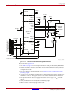
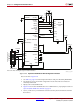
In x4 mode, the Fast-Read Quad Output (6Bh) instruction is issued and is similar to the
standard Fast Read (0Bh) instruction except that data is output on four data pins, instead
of just DO. This allows data to be transferred from the quad output at four times the rate of
standard SPI devices. The timing diagram of the Master Serial SPI configuration mode
using an SPI flash with quad read bit command (6Bh) is shown in Figure 2-18.
Power-On Sequence Precautions
At power-on, the FPGA automatically starts its configuration procedure. When the FPGA
is in Master Serial SPI configuration mode, the FPGA asserts CSO_B Low to select the SPI
flash and drives a read command to the SPI flash. The SPI flash must be awake and ready
to receive commands before the FPGA drives CSO_B Low and sends the read command.
Because different power rails can supply the FPGA and SPI flash or because the FPGA and
SPI flash can respond at different times along the ramp of a shared power supply, special
attention to the FPGA and SPI Flash power-on sequence or power-on ramps is essential.
The power-on sequence or power supply ramps can cause the FPGA to awake, or start,
before the SPI flash or vice versa. In addition, some SPI flash devices specify a minimum
time period, which can be several milliseconds from power-on, during which the device
must not be selected. For many systems with near-simultaneous power supply ramps, the
FPGA power-on reset time (T
POR
) can sufficiently delay the start of the FPGA
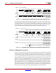
X-Ref Target - Figure 2-17
Figure 2-17: Timing Diagram of Winbond SPI Dual-Read Bit Command (3Bh)
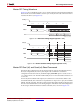
X-Ref Target - Figure 2-18
Figure 2-18: Timing Diagram of Winbond SPI Quad-Read Bit Command (6Bh)
CSO_B
CCLK
Read Command 24-Bit Address
Dummy
Byte (8 Bits)
MOSI/
MISO[0]
DIN/
MISO[1]
UG380_c2_17_052009
D6 D4 D2 D0
D7 D5 D3 D1
Data Byte 1
CSO_B
Read Command 24-Bit Address D4 D0 D4 D0
D5 D1 D5 D1
D6 D2 D6 D2
D7 D3 D7 D3
Dummy
Byte (8 Bits)
CCLK
MOSI/
MISO[0]
DIN/
MISO[1]
MISO[2]
MISO[3]
UG380_c2_18_052009
D0–D7
Data Byte 1 This corresponds with the first two columns of data.
Next D0–D7
Data Byte 2 This corresponds with the last two columns of data.