
User guide

42 www.xilinx.com Spartan-6 FPGA Configuration User Guide
UG380 (v2.7) October 29, 2014
Chapter 2: Configuration Interface Basics
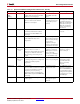
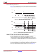
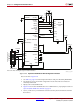
Notes relevant to Figure 2-12:
1. See Table 5-2, page 72 for internal pin terminations and pins affected by HSWAPEN.
2. DOUT should be connected to the DIN of the downstream FPGA for daisy-chained
configuration modes.
3. For more details on CCLK termination, see Board Layout for Configuration Clock
(CCLK), page 54.
4. A series resistor should be considered for the datapath from the flash to the FPGA to
minimize overshoot. The proper resistor value can be determined from simulation.
5. The Spartan-6 FPGA VCCO_2 supply must be the same voltage as V
CC
of the SPI
device.
6. CSO_B and MOSI are clocked by the CCLK falling edge.
7. DIN is clocked on the rising edge of the CCLK.
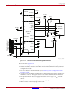
X-Ref Target - Figure 2-12
Figure 2-12: Spartan-6 FPGA SPI Configuration Interface
UG380_c2_12_062510
VCCINT
CSO_B
VCCO_2
INIT_B
DIN
MOSI
D
S
VCC
Q
C
GND
HSWAPEN
VCCO_0
CCLK
VCCO_1
Numonyx
M25Pxx
SPI Flash
HOLD
M1
M0
DOUT
W
TMS
TDO
TCK
TDI
VCCAUX
Spartan-6
FPGA
DONE
GND
PROGRAM_B
VREF
TMS
TCK
TDO
TDI
N.C.
N.C.
1
14
Xilinx Cable Header
(JTAG Interface)
PROGRAM_B
VCCO_2
2.4 kΩ
4.7 kΩ
330Ω
4.7 kΩ
VCCO_0
VCCO_1
VCCO_2
VCCO_2
VCCO_2
VCCO_2
VCCO_2
Refer to the Notes following this figure for related information.
VCCAUX
VCCAUX
VFS
VBATT
VFS
VBATT
SUSPEND