
User guide

40 www.xilinx.com Spartan-6 FPGA Configuration User Guide
UG380 (v2.7) October 29, 2014
Chapter 2: Configuration Interface Basics
SPI Configuration Interface
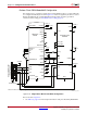
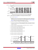
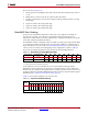
The Master Serial Peripheral Interface (SPI) (Figure 2-11) allows a SPI serial flash to be used
to store configuration data. The Spartan-6 FPGA configures itself from a directly attached
industry-standard SPI serial flash PROM. Although SPI is a standard four-wire interface,
various available SPI flash memories use different read commands and protocol.
Figure 2-12 shows the connections for an SPI configuration with a data width of x1 or x2.
These connections are the same because the x2 flash devices use the D pin as a dual
purpose Data In/Out pin. Connections for the SPI x4 option are shown in Figure 2-13,
page 43; two additional data pins provide a 4-bit data interface. Daisy-chained
configuration mode is only available in SPI x1 mode. The FPGA pin connections to the SPI
flash PROM involved in the Master SPI mode are listed in Table 2-5.
The iMPACT programming software provides the ability to program an SPI serial flash
using an indirect programming method. This downloads a new FPGA design that
provides a connection from the iMPACT software through the Spartan-6 device to the SPI
flash. Previous FPGA memory contents are lost. For a list of supported SPI flash devices in
the latest version of software, see the software help documentatio
n.
For more details see XAPP586
: Using SPI Flash with 7 Series FPGAs.
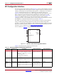
Table 2-6 describes the SPI configuration interface pins.
X-Ref Target - Figure 2-11
Figure 2-11: Spartan-6 FPGA SPI Configuration Interface
DONE
CCLK
PROGRAM_B
INIT_B
DIN
M[1:0]
UG380_c2_11_051909
MOSI
CSO_B
Table 2-6: Spartan-6 FPGA SPI Configuration Interface Pins
Pin Name FPGA Direction Description During Configuration After Configuration
HSWAPEN Input User I/O Pull-Up Control.
When Low during configuration, enables
pull-up resistors in all I/O pins to respective
I/O bank V
CCO
input.
0: Pull-ups during configuration
1: No pull-ups
Drive at valid level
throughout configuration.
User I/O
M[1:0] Input Mode Select.
Selects the FPGA configuration mode.
M[1:0] = 2'b01
Sampled when INIT_B goes
High.
User I/O
MOSI/
MISO[0]/
CSI_B
Output/Input Master FPGA Serial Data Output and
Master FPGA Serial Data Input.
Connect to the SPI Flash PROM’s Slave Data
Input pin.
FPGA sends SPI flash
memory read commands
and starting address to the
PROM’s serial data input.
User I/O