
User guide

Spartan-6 FPGA Configuration User Guide www.xilinx.com 33
UG380 (v2.7) October 29, 2014
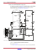
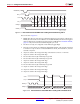
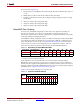
SelectMAP Configuration Interface
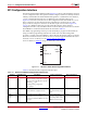
2. The CCLK net requires Thevenin parallel termination. For more details, see Board
Layout for Configuration Clock (CCLK), page 54.
3. The DONE pin is by default an open-drain output with an internal pull-up. An
additional external pull-up is recommended. The DONE pin has a programmable
active driver that can be enabled via the BitGen option -g DriveDone.
4. A series resistor should be considered for the datapath from the flash to the FPGA to
minimize overshoot. The proper resistor value can be determined from simulation.
5. The INIT_B pin is a bidirectional, open-drain pin. An external pull-up resistor is
recommended.
6. The BitGen startup clock setting must be set for CCLK for SelectMAP configuration.
7. The PROM in this diagram represents one or more Xilinx PROMs. Multiple PROMs
can be cascaded to increase the overall configuration storage capacity.
8. The
BIT file must be reformatted into a PROM file before it can be stored on the
PROM. Refer to the Generating PROM Files, page 77.
9. On some Xilinx PROMs, the reset polarity is programmable. RESET
should be
configured as active Low when using this setup.
10. The Xilinx PROM must be set for parallel mode. This mode is not available for all
devices.
11. When configuring a Spartan-6 device in SelectMAP mode from a Xilinx configuration
PROM, the RDWR_B and CSI_B signals can be tied Low (see SelectMAP Data Loading,
page 35).
12. The D bus can be x8 or x16 for Master SelectMAP configuration. The maximum data
width for XCFxxP is x8.
13. Platform Flash PROM SelectMAP configuration is specific to the Platform Flash XCFP
PROM only. The Platform Flash XCFS PROM only supports serial configuration
modes.
14. The address bus A[25:0] along with the BUSY, FOE_B, FCS_B, and FWE_B pins toggle
during configuration. The system should be able to handle activity on these dual-
purpose pins during the configuration process.
15. The Spartan-6 FPGA VCCO_2 supply input and the Platform Flash PROM V
CCO
supply input must be the same voltage.
16. V
FS
is present in 6SLX75/T, 6SLX100/T, and 6SLX150/T devices, and is used for
eFUSE programming. See eFUSE, page 91 for more details.
17. V
BATT
is present in 6SLX75/T, 6SLX100/T, and 6SLX150/T devices, and is the power
source for AES key storage. If AES encryption is unused, V
BATT
can be tied to either
V
CCAUX
or ground, or left unconnected.
18. If VCCO_2 is 1.8V, V
CCAUX
must be 2.5V. If VCCO_2 is 2.5V or 3.3V, V
CCAUX
can be
either 2.5V or 3.3V.
19. The SUSPEND pin should be Low during power up and configuration. If the Suspend
feature is not used, the SUSPEND pin must be connected to ground.