
User guide


Spartan-6 FPGA Configuration User Guide www.xilinx.com 161
UG380 (v2.7) October 29, 2014
JTAG Configuration/Readback
3. Overwrite the FPGA configuration with a design that does not use inversion at the
inputs.
4. Modify the original design to avoid the IOB invert path.
JSTART and JSHUTDOWN are instructions specific to the Spartan-6 architecture and
configuration flow. In Spartan-6 devices, the TAP controller is not reset by the
PROGRAM_B pin and can only be reset by bringing the controller to the TLR state. The
TAP controller is reset on power up.
For details on the standard boundary-scan instructions EXTEST, INTEST, and BYPASS,
refer to IEEE Std 1149.1.
Boundary-Scan Architecture
Spartan-6 device registers include all registers required by IEEE Std 1149.1. In addition to
the standard registers, the family contains optional registers for simplified testing and
verification (Table 10-1).
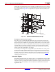
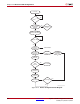
Boundary-Scan Register
The test primary data register is the boundary-scan register. Boundary-scan operation is
independent of individual IOB configuration. Each IOB, bonded or unbonded, starts as
bidirectional with 3-state control. Later, it can be configured to be an input, output, or
3-state only. Therefore, three data register bits are provided per IOB (Figure 10-1).
When conducting a data register (DR) operation, the DR captures data in a parallel fashion
during the CAPTURE-DR state. The data is then shifted out and replaced by new data
during the SHIFT-DR state. For each bit of the DR, an update latch is used to hold the input
data stable during the next SHIFT-DR state. The data is then latched during the
UPDATE-DR state when TCK is Low.
The update latch is opened each time the TAP controller enters the UPDATE-DR state. Care
is necessary when exercising an INTEST or EXTEST to ensure that the proper data has been
latched before exercising the command. This is typically accomplished by using the
SAMPLE instruction.
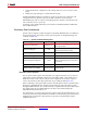
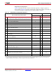
Table 10-1: Spartan-6 FPGA JTAG Registers
Register Name Register Length Description
Boundary-Scan Register 3 bits per I/O
Controls and observes input, output,
and output enable
Instruction Register 6 bits
Holds current instruction opcode and
captures internal device status
BYPASS Register 1 bit Bypasses the device
Identification Register 32 bits Captures the Device ID
JTAG Configuration Register 16 bits
Allows access to the configuration bus
when using the CFG_IN or CFG_OUT
instructions
USERCODE Register 32 bits Captures the user-programmable code
User-Defined Registers (USER1,
USER2, USER3, and USER4)
Design specific Design specific