
User guide

Spartan-6 FPGA Configuration User Guide www.xilinx.com 105
UG380 (v2.7) October 29, 2014
Configuration Packets
Configuration Watchdog Timer Register
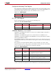
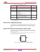
The configuration watchdog timer (CWDT) register stores the value of the number of clock
cycles that the FPGA will wait before the watchdog time-out (in which SYNCWORD is not
received). The default is 64k clock cycles. The minimum value is 16h'0201.
HC_OPT_REG Register
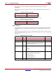
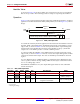
The HC_OPT_REG register can only be reset to default by por_b.
GENERAL Registers 1, 2, 3, 4, and 5
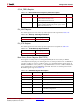
GENERAL1 and GENERAL2 registers are used to store loadable multiple configuration
addresses for SPI and BPI.
GENERAL3 and GENERAL4 registers have a similar function as GENERAL1 and
GENERAL2, except that GENERAL3 and GENERAL4 store the golden bitstream address
instead of the MultiBoot address.
The GENERAL5 register is a 16-bit register that allows users to store and access any extra
information desired for the fail-safe scheme. These register contents are untouched during
a soft reboot.
These registers are set by the bitstream. BitGen can be instructed not to write to these
registers using the -g next_config_register_write:Disable command. This allows the ability
to store user data in the FPGA between re-configuration attempts.
If the second configuration needs a previously unknown SPI vendor command, the new
vendor command has already been loaded in GENERAL2 from the bitstream by this point.
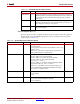
Table 5-39: CWDT Register
Bits Value
[15:0] 16h'ffff
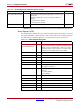
Table 5-40: HC_OPT_REG Description
Name Bits Description Default
INIT_SKIP 6 0: Do not skip initialization.
1: Skip initialization.
0
RESERVED 5:0 Reserved. 011111
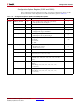
Table 5-41: General Registers
Name Bits Description
GENERAL1 [15:0] The lower half of the multiple boot address.
GENERAL2 [15:0]
15:8 – SPI opcode.
7:0 – Higher half of the boot address.
GENERAL3 [15:0] The lower half of the golden bitstream address.
GENERAL4 [15:0]
15:8 – SPI opcode.
7:0 – Higher half of the golden boot address.
GENERAL5 [15:0] The user-defined scratchpad register.