
Service manual


STP 11-25R13-SM-TG
O - 2
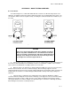
In a positive or negative diode clamper with zero reference level (Figure O-1), if the resistor or diode
were to short there would be no output. If the capacitor were to short, the circuit would act as a half-wave
rectifier. An open in the diode would cause the output to appear with equal parts of the waveform above
and below a zero reference.
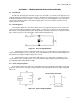
Figure O-1. Positive Diode Clamper with Zero Reference Level
a. A square wave is applied to the coupling circuit of C and R. The square wave may be at any
DC level. Any DC level that may be present will be blocked by capacitor C. The negative half-cycle is
shown first for simplicity of description only.
(1) Initially the topside of C is at zero volts. When the negative half-cycle is coupled across C, the
diode becomes forward-biased. Because the resistance of the diode is very small, current through the
diode prevents the output terminal from going negative.
(2) Electrons are repelled from the top plate of C, effectively charging C to the peak value of the
input square wave. The E
c
waveform shows the rapid charge of C. When C is charged, the output
voltage level is zero volt. As shown in Figure O-1, C charges to +5V. This action occurs from Tl to T2.
b. At T2 the waveform changes polarity, from -5V to +5V, or a 10V positive charge. The +10V
charge couples across C reverse-biases the diode and it becomes an open. C attempts to discharge
through R, but the time constant is long and the charge on C remains almost constant from T2 to T3.
From T2 to T3 the output waveform is at +10 volts (+5V charge on C plus the 5V peak of the waveform).
c. On the next negative half-cycle, from T3 to T4, the charge remaining on C holds the diode cutoff
until the negative peak exceeds E
c
. The diode conducts for a short period to recharge C to the peak
value (+5V). The discharge time constant is long so C only loses a very small part of its charge. The
recharging current causes the small changes on E
out
and E
c
at T3.
d. An open in the diode will effectively eliminate the diode from the circuit. This will change the
reference so that the input will be equally divided across whatever reference voltage is present from the
bias power source.
e. A short in the diode will effectively eliminate both the resistor and the diode from the circuit and
the output will remain at a DC level. When this condition occurs it may be hard to verify due to the
internal resistance of the power source; therefore, the circuit should be isolated and each component
checked.
O-5. Positive Diode Clamping with Bias Applied.